|
数据搜索系统,热门电子元器件搜索 |
|
|
数据搜索系统,热门电子元器件搜索 |
|
MAX5500AGAP+ 数据表(PDF) 13 Page - Maxim Integrated Products |
|
|
|||||||||||||||||||||||||||||
MAX5500AGAP+ 数据表(HTML) 13 Page - Maxim Integrated Products |
|
|
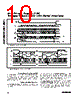
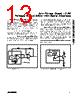
13 / 15 page  Low-Power, Quad, 12-Bit Voltage-Output DACs with Serial Interface ______________________________________________________________________________________ 13 Digitally Programmable Current Source The circuit of Figure 12 places an npn transistor (2N3904 or similar) within the op-amp feedback loop to implement a digitally programmable, unidirectional cur- rent source. This circuit drives 4mA to 20mA current loops, which are commonly used in industrial-control applications. The output current is calculated with the following equation: IOUT = (VREF/R) x (NB/4096) where NB is the numeric value of the DAC’s binary input code and R is the sense resistor shown in Figure 12. Power-Supply Considerations On power-up, all input and DAC registers are cleared (set to zero code) and DOUT is in mode 0 (serial data is shifted out of DOUT on the clock’s falling edge). For rated MAX5500/MAX5501 performance, limit VREFAB/ VREFCD to 1.4V below VDD. Bypass VDD with a 4.7µF capacitor in parallel with a 0.1µF capacitor to AGND. Use short lead lengths and place the bypass capaci- tors as close as possible to the supply inputs. Grounding and Layout Considerations Digital or AC transient signals between AGND and DGND create noise at the analog outputs. Connect AGND and DGND together at the DAC, and then con- nect this point to the highest-quality ground available. Good PCB ground layout minimizes crosstalk between DAC outputs, reference inputs, and digital inputs. Reduce crosstalk by keeping analog lines away from digital lines. Do not use wire-wrapped boards. Chip Information PROCESS: BiCMOS DAC VOUT +5V -5V R1 = R2 = 10kΩ ± 0.1% MAX5500 MAX5501 REF_ R1 R2 FB_ OUT_ Figure 11. Bipolar Output Circuit DAC_ MAX5500 MAX5501 REF_ OUT_ R IOUT 2N3904 VL FB_ Figure 12. Digitally Progammable Current Source |
|
|
链接网址 |
| ALLDATASHEET是否为您带来帮助? [ DONATE ] |
关于 Alldatasheet | 广告服务 | 联系我们 | 隐私政策 | 数据表链接 | 链接交换 | 制造商名单 All Rights Reserved©Alldatasheet.com |
| Russian : Alldatasheetru.com | Korean : Alldatasheet.co.kr | Spanish : Alldatasheet.es | French : Alldatasheet.fr | Italian : Alldatasheetit.com Portuguese : Alldatasheetpt.com | Polish : Alldatasheet.pl | Vietnamese : Alldatasheet.vn Indian : Alldatasheet.in | Mexican : Alldatasheet.com.mx | British : Alldatasheet.co.uk | New Zealand : Alldatasheet.co.nz |
|
Family Site : ic2ic.com |
icmetro.com |
 Chinese ▼
 English
 Chinese
 German
 Japanese
 Russian
 Korean
 Spanish
 French
 Italian
 Portuguese
 Polish
 Vietnamese
 Indian
 Mexican
 British
 New Zealand