|
数据搜索系统,热门电子元器件搜索 |
|
|
数据搜索系统,热门电子元器件搜索 |
|
ICS8735-21 数据表(PDF) 2 Page - Integrated Device Technology |
|
|
|||||||||||||||||||||||||||||
ICS8735-21 数据表(HTML) 2 Page - Integrated Device Technology |
|
|
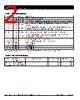
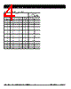
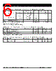
2 / 20 page  ICS8735-21 700MHZ, DIFFERENTIAL-TO-3.3V LVPECL ZERO DELAY CLOCK GENERATOR IDT™ / ICS™ 3.3V LVPECL ZERO DELAY CLOCK GENERATOR 2 ICS8735AM-21 REV. A JULY 31, 2008 Table 1. Pin Descriptions NOTE: Pullup and Pulldown refer to internal input resistors. See Table 2, Pin Characteristics, for typical values. Table 2. Pin Characteristics Name Type Description CLK Input Pulldown Non-inverting differential clock input. nCLK Input Pullup Inverting differential clock input. nFB_IN Input Pullup Inverting differential feedback input to phase detector for regenerating clocks with “zero delay.” FB_IN Input Pulldown Non-inverted differential feedback input to phase detector for regenerating clocks with “zero delay.” MR Input Pulldown Active HIGH Master Reset. When logic HIGH, the internal dividers are reset causing the true output Q to go low and the inverted output nQ to go high. When logic LOW, the internal dividers and the outputs are enabled. LVCMOS / LVTTL interface levels. SEL0, SEL1, SEL2, SEL3 Input Pulldown Determines output divider values in Table 3. LVCMOS / LVTTL interface levels. PLL_SEL Input Pullup PLL select. Selects between the PLL and reference clock as the input to the dividers. When LOW, selects reference clock. When HIGH, selects PLL. LVCMOS/LVTTL interface levels. nQ, Q Output Differential output pair. LVPECL interface levels. nQFB, QFB Output Differential feedback output pair. LVPECL interface levels. VEE Power Negative supply pin. VCC Power Core supply pins. VCCA Power Analog supply pin. VCCO Power Output supply pin. Symbol Parameter Test Conditions Minimum Typical Maximum Units CIN Input Capacitance 4 pF RPULLUP Input Pullup Resistor 51 k Ω RPULLDOWN Input Pulldown Resistor 51 k Ω |
|
|
链接网址 |
| ALLDATASHEET是否为您带来帮助? [ DONATE ] |
关于 Alldatasheet | 广告服务 | 联系我们 | 隐私政策 | 数据表链接 | 链接交换 | 制造商名单 All Rights Reserved©Alldatasheet.com |
| Russian : Alldatasheetru.com | Korean : Alldatasheet.co.kr | Spanish : Alldatasheet.es | French : Alldatasheet.fr | Italian : Alldatasheetit.com Portuguese : Alldatasheetpt.com | Polish : Alldatasheet.pl | Vietnamese : Alldatasheet.vn Indian : Alldatasheet.in | Mexican : Alldatasheet.com.mx | British : Alldatasheet.co.uk | New Zealand : Alldatasheet.co.nz |
|
Family Site : ic2ic.com |
icmetro.com |
 Chinese ▼
 English
 Chinese
 German
 Japanese
 Russian
 Korean
 Spanish
 French
 Italian
 Portuguese
 Polish
 Vietnamese
 Indian
 Mexican
 British
 New Zealand