|
数据搜索系统,热门电子元器件搜索 |
|
|
数据搜索系统,热门电子元器件搜索 |
|
74ACT715-RSC 数据表(PDF) 5 Page - Fairchild Semiconductor |
|
|
|||||||||||||||||||||||||||||
74ACT715-RSC 数据表(HTML) 5 Page - Fairchild Semiconductor |
|
|
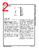
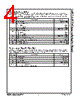
5 / 18 page  ©1988 Fairchild Semiconductor Corporation www.fairchildsemi.com 74ACT715, 74ACT715-R Rev. 1.3 5 Register Description All of the data registers are 12 bits wide. Width’s of all pulses are defined by specifying the start count and end count of all pulses. Horizontal pulses are specified with respect to the number of clock pulses per line and verti- cal pulses are specified with respect to the number of lines per frame. REG0—Status Register The Status Register controls the mode of operation, the signals that are output and the polarity of these outputs. The default value for the Status Register is 0 (000 Hex) for the ACT715 and is “1024” (400 Hex) for the ACT715-R. Bits 0–2 Bits 3–4 Double Equalization and Serration mode will output equalization and serration pulses at twice the HSYNC frequency (i.e., 2 equalization or serration pulses for every HSYNC pulse). Single Equalization and Serration mode will output an equalization or serration pulse for every HSYNC pulse. In Interlaced mode equalization and serration pulses will be output during the VBLANK period of every odd and even field. Interlaced Single Equalization and Serration mode is not possible with this part. Bits 5–8 Bits 5 through 8 control the polarity of the outputs. A value of zero in these bit locations indicates an output pulse active LOW. A value of 1 indicates an active HIGH pulse. B5— VCBLANK Polarity B6— VCSYNC Polarity B7— HBLHDR Polarity B8— HSYNVDR Polarity Bits 9–11 Bits 9 through 11 enable several different features of the device. B9— Enable Equalization/Serration Pulses (0) Disable Equalization/Serration Pulses (1) B10— Disable System Clock (0) Enable System Clock (1) Default values for B10 are “0” in the ACT715 and “1” in the ACT715-R. B11— Disable Counter Test Mode (0) Enable Counter Test Mode (1) This bit is not intended for the user but is for internal testing only. Horizontal Interval Registers The Horizontal Interval Registers determine the number of clock cycles per line and the characteristics of the Horizontal Sync and Blank pulses. REG1— Horizontal Front Porch REG2— Horizontal Sync Pulse End Time REG3— Horizontal Blanking Width REG4— Horizontal Interval Width # of Clocks per Line Vertical Interval Registers The Vertical Interval Registers determine the number of lines per frame, and the characteristics of the Vertical Blank and Sync Pulses. REG5— Vertical Front Porch REG6— Vertical Sync Pulse End Time REG7— Vertical Blanking Width REG8— Vertical Interval Width # of Lines per Frame Equalization and Serration Pulse Specification Registers These registers determine the width of equalization and serration pulses and the vertical interval over which they occur. REG 9— Equalization Pulse Width End Time REG10— Serration Pulse Width End Time REG11— Equalization/Serration Pulse Vertical Interval Start Time REG12— Equalization/Serration Pulse Vertical Interval End Time Vertical Interrupt Specification Registers These Registers determine the width of the Vertical Interrupt signal if used. REG13— Vertical Interrupt Activate Time REG14— Vertical Interrupt Deactivate Time B2 B1 B0 VCBLANK VCSYNC HBLHDR HSYNVDR 0 0 0 CBLANK CSYNC HGATE VGATE (DEFAULT) 0 0 1 VBLANK CSYNC HBLANK VGATE 0 1 0 CBLANK VSYNC HGATE HSYNC 0 1 1 VBLANK VSYNC HBLANK HSYNC 1 0 0 CBLANK CSYNC CUSOR VINT 1 0 1 VBLANK CSYNC HBLANK VINT 1 1 0 CBLANK VSYNC CUSOR HSYNC 1 1 1 VBLANK VSYNC HBLANK HSYNC B4 B3 Mode of Operation 0 0 Interlaced Double Serration and Equalization (DEFAULT) 0 1 Non Interlaced Double Serration 1 0 Illegal State 1 1 Non Interlaced Single Serration and Equalization |
|
|
链接网址 |
| ALLDATASHEET是否为您带来帮助? [ DONATE ] |
关于 Alldatasheet | 广告服务 | 联系我们 | 隐私政策 | 数据表链接 | 链接交换 | 制造商名单 All Rights Reserved©Alldatasheet.com |
| Russian : Alldatasheetru.com | Korean : Alldatasheet.co.kr | Spanish : Alldatasheet.es | French : Alldatasheet.fr | Italian : Alldatasheetit.com Portuguese : Alldatasheetpt.com | Polish : Alldatasheet.pl | Vietnamese : Alldatasheet.vn Indian : Alldatasheet.in | Mexican : Alldatasheet.com.mx | British : Alldatasheet.co.uk | New Zealand : Alldatasheet.co.nz |
|
Family Site : ic2ic.com |
icmetro.com |
 Chinese ▼
 English
 Chinese
 German
 Japanese
 Russian
 Korean
 Spanish
 French
 Italian
 Portuguese
 Polish
 Vietnamese
 Indian
 Mexican
 British
 New Zealand