|
数据搜索系统,热门电子元器件搜索 |
|
|
数据搜索系统,热门电子元器件搜索 |
|
STLQ50C-R 数据表(PDF) 10 Page - STMicroelectronics |
|
|
|||||||||||||||||||||||||||||
STLQ50C-R 数据表(HTML) 10 Page - STMicroelectronics |
|
|
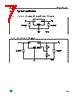
10 / 18 page  Application information STLQ50XX 10/18 7 Application information The STLQ50 is a BiCMOS linear regulator specifically designed for operating in environment with very low power consumption constraints. The very low quiescent current of 3 µA is obtained with use of CMOS technology that makes the device suitable for those application that have very long stand-by time. The very low power consumption allows extending the battery life and the tiny packages (SOT323-5L or SOT23-5L) fulfil the space saving requirements of battery powered equipments. Moreover the STLQ50 provides wide input voltage operation from 2.5 V up to 12 V. The P-MOS pass element allows also a very good drop-out figure: 0.7 V at full load and at 125 °C without affecting the consumption characteristics. 7.1 External components The typical application schematic of STLQ50 is shown in Figure 1 - Figure 2, a 1 µF input and output capacitors placed close to the device are needed in order to provide proper operation. The device is stable with electrolytic and ceramic output capacitors having values higher than 1 µF (see figure typical characteristics for stability details). In the adjustable version (STLQ50) the output voltage is programmed using an external resistor divider as shown in Figure 2. The output voltage can be adjusted from 1.22 to 11 V and it can be calculated using the following formula: VO = VFB x (1+R1/R2) where VFB=1.222 V is the internal reference voltage; The sum between R1 and R2 resistors should be chosen in order to guarantee 1 µA of divider current at least. Lower value resistors will improve the noise performances but the quiescent current will increase. Higher value resistors should be avoided because the ADJ leakage current will influence the voltage set by the resistor divider making the above formula no more valid. The suggested design procedure is to choose R2 = 1 MΩ and then calculate R1 using the following formula: R1 = (VO/VFB-1) x R2 7.2 Power dissipation In order to ensure proper operation, the STLQ50 junction temperature should never exceed 125 °C, this limits the maximum power dissipation the regulator can sustain in any application. The maximum power dissipation can be calculated as: PDMAX = (TJMAX - TA)/RthJA where TJMAX = 125 °C; TA is the ambient temperature; RthJA is the junction to ambient thermal resistance of the package (seeTable 4 thermal data). The power dissipation can be calculated simply as: PD = (VI - VO) x IO In every application condition, PD must be lower than PDMAX. |
|
|
链接网址 |
| ALLDATASHEET是否为您带来帮助? [ DONATE ] |
关于 Alldatasheet | 广告服务 | 联系我们 | 隐私政策 | 数据表链接 | 链接交换 | 制造商名单 All Rights Reserved©Alldatasheet.com |
| Russian : Alldatasheetru.com | Korean : Alldatasheet.co.kr | Spanish : Alldatasheet.es | French : Alldatasheet.fr | Italian : Alldatasheetit.com Portuguese : Alldatasheetpt.com | Polish : Alldatasheet.pl | Vietnamese : Alldatasheet.vn Indian : Alldatasheet.in | Mexican : Alldatasheet.com.mx | British : Alldatasheet.co.uk | New Zealand : Alldatasheet.co.nz |
|
Family Site : ic2ic.com |
icmetro.com |
 Chinese ▼
 English
 Chinese
 German
 Japanese
 Russian
 Korean
 Spanish
 French
 Italian
 Portuguese
 Polish
 Vietnamese
 Indian
 Mexican
 British
 New Zealand