|
数据搜索系统,热门电子元器件搜索 |
|
|
数据搜索系统,热门电子元器件搜索 |
|
RT8205A 数据表(PDF) 7 Page - Richtek Technology Corporation |
|
|
|||||||||||||||||||||||||||||
RT8205A 数据表(HTML) 7 Page - Richtek Technology Corporation |
|
|
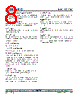
7 / 28 page  RT8205A/B/C 7 DS8205A/B/C-06 July 2012 www.richtek.com © Copyright 2012 Richtek Technology Corporation. All rights reserved. is a registered trademark of Richtek Technology Corporation. Functional Pin Description ENTRIP1 (Pin 1) Channel 1 enable and Current Limit setting Input. Connect resistor to GND to set the threshold for channel 1 synchronous RDS(ON) sense. The GND-PHASE1 current- limit threshold is 1/10th the voltage seen at ENTRIP1 over a 0.5V to 2V range. There is an internal 10uA current source from VREG5 to ENTRIP1. The logic current limit threshold is default to 200mV value if ENTRIP1 is higher than VREG5-1V. FB1 (Pin 2) SMPS1 Feedback Input. Connect FB1 to VREG5 or GND for fixed 5V operation. Or connect FB1 to a resistive voltage- divider from VOUT1 to GND to adjust output from 2V to 5.5V. REF (Pin 3) 2V Reference Output. Bypass to GND with a 0.22uF capacitor. REF can source up to 50uA for external loads. Loading REF degrades FBx and output accuracy according to the REF load-regulation error. TONSEL (Pin 4) Frequency Selectable Input for VOUT1/VOUT2 respectively. 400kHz/500kHz : Connect to VREG5 or VREG3 300kHz/375kHz : Connect to REF 200kHz/250kHz : Connect to GND FB2 (Pin 5) SMPS2 Feedback Input. Connect FB2 to VREG5 or GND for fixed 3.3V operation. Or connect FB2 to a resistive voltage-divider from VOUT2 to GND to adjust output from 2V to 5.5V. ENTRIP2 (Pin 6) Channel 2 enable and Current Limit setting Input. Connect resistor to GND to set the threshold for channel 2 synchronous RDS(ON) sense. The GND-PHASE2 current- limit threshold is 1/10th the voltage seen at ENTRIP2 over a 0.5V to 2V range. There is an internal 10uA current source from VREG5 to ENTRIP2. The logic current limit threshold is default to 200mV value if ENTRIP2 is higher than VREG5-1V. VOUT2 (Pin 7) SMPS2 Output Voltage-Sense Input. Connect to the SMPS2 output. VOUT2 is an input to the on-time one- shot circuit. It also serves as the SMPS2 feedback input in fixed-voltage mode. VREG3 (Pin 8) 3.3V Linear Regulator Output. BOOT2 (Pin 9) Boost Flying Capacitor Connection for SMPS2. Connect to an external capacitor according to the typical application circuits. UGATE2 (Pin 10) High-Side MOSFET Floating Gate-Driver Output for SMPS2. UGATE2 swings between PHASE2 and BOOT2. PHASE2 (Pin 11) Inductor Connection for SMPS2. PHASE2 is the internal lower supply rail for the UGATE2 high-side gate driver. PHASE2 is also the current-sense input for the SMPS2. LGATE2 (Pin 12) SMPS2 Synchronous-Rectifier Gate-Drive Output. LGATE2 swings between GND and VREG5. EN (Pin 13) Master Enable Input. The REF/VREG5/VREG3 are enabled if it is within logic high level and disable if it is less than the logic low level. SKIPSEL (Pin 14) Operation Mode Selectable Input. Ultrasonic Mode : Connect to VREG5 or VREG3 Diode Emulation Mode : Connect to REF PWM Mode : Connect to GND |
|
|
链接网址 |
| ALLDATASHEET是否为您带来帮助? [ DONATE ] |
关于 Alldatasheet | 广告服务 | 联系我们 | 隐私政策 | 数据表链接 | 链接交换 | 制造商名单 All Rights Reserved©Alldatasheet.com |
| Russian : Alldatasheetru.com | Korean : Alldatasheet.co.kr | Spanish : Alldatasheet.es | French : Alldatasheet.fr | Italian : Alldatasheetit.com Portuguese : Alldatasheetpt.com | Polish : Alldatasheet.pl | Vietnamese : Alldatasheet.vn Indian : Alldatasheet.in | Mexican : Alldatasheet.com.mx | British : Alldatasheet.co.uk | New Zealand : Alldatasheet.co.nz |
|
Family Site : ic2ic.com |
icmetro.com |
 Chinese ▼
 English
 Chinese
 German
 Japanese
 Russian
 Korean
 Spanish
 French
 Italian
 Portuguese
 Polish
 Vietnamese
 Indian
 Mexican
 British
 New Zealand