|
数据搜索系统,热门电子元器件搜索 |
|
|
数据搜索系统,热门电子元器件搜索 |
|
AD8564AR 数据表(PDF) 5 Page - Analog Devices |
|
|
|||||||||||||||||||||||||||||
AD8564AR 数据表(HTML) 5 Page - Analog Devices |
|
|
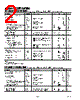
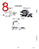
5 / 8 page  AD8564 –5– REV. A V+DIG SUPPLY VOLTAGE – V 3.000 2.500 0.000 24 12 68 10 2.000 1.500 1.000 0.500 TA = +25 C TA = +85 C TA = –40 C Figure 10. I+DIG: Digital Supply Cur- rent/Comparator vs. Supply Voltage TEMPERATURE – C 2.000 1.500 0.000 –75 –50 150 –25 0 25 75 100 125 50 1.000 0.500 Figure 13. I+DIG: Digital Supply Current/ Comparator vs. Temperature APPLICATIONS OPTIMIZING HIGH SPEED PERFORMANCE As with any high speed comparator or amplifier, proper design and layout techniques should be used to ensure optimal perfor- mance from the AD8564. The performance limits of high speed circuitry can easily be a result of stray capacitance, improper ground impedance or other layout issues. Minimizing resistance from source to the input is an important consideration in maximizing the high speed operation of the AD8564. Source resistance in combination with equivalent input capacitance could cause a lagged response at the input, thus delaying the output. The input capacitance of the AD8564 in combination with stray capacitance from an input pin to ground could result in several picofarads of equivalent capaci- tance. A combination of 3 k Ω source resistance and 5 pF of input capacitance yields a time constant of 15 ns, which is slower than the 5 ns capability of the AD8564. Source imped- ances should be less than 1 k Ω for the best performance. It is also important to provide bypass capacitors for the power supply in a high speed application. A 1 µF electrolytic bypass capacitor should be placed within 0.5 inches of each power supply pin to ground. These capacitors will reduce any potential voltage ripples from the power supply. In addition, a 10 nF ceramic capacitor should be placed as close as possible from the power supply pins to ground. These capacitors act as a charge reservoir for the device during high frequency switching. A ground plane is recommended for proper high speed perfor- mance. This can be created by using a continuous conductive plane over the surface of the circuit board, only allowing breaks in the plane for necessary current paths. The ground plane provides a low inductance ground, eliminating any potential differences at different ground points throughout the circuit board caused from “ground bounce.” A proper ground plane also minimizes the effects of stray capacitance on the circuit board. OUTPUT LOADING CONSIDERATIONS The AD8564 output can deliver up to 40 mA of output current without any significant increase in propagation delay. The out- put of the device should not be connected to more than twenty (20) TTL input logic gates, or drive a load resistance less than 100 Ω. To ensure the best performance from the AD8564 it is impor- tant to minimize capacitive loading of the output of the device. Capacitive loads greater than 50 pF will cause ringing on the output waveform and will reduce the operating bandwidth of the comparator. Propagation delay will also increase with capacitive loads above 100 pF. TEMPERATURE – C 0.000 –1.000 –5.000 –75 –50 150 –25 0 25 75 100 125 50 –2.000 –3.000 –4.000 V+ANA = 5V V+ANA = +5V Figure 12. I–ANA: Analog Supply Cur- rent/Comparator vs. Temperature TEMPERATURE – C 5.000 4.000 0 –75 –50 150 –25 0 25 75 100 125 50 3.000 2.000 1.000 V+ANA = 5V V+ANA = +5V Figure 11. I+ANA: Analog Supply Cur- rent/Comparator vs. Temperature |
|
|
链接网址 |
| ALLDATASHEET是否为您带来帮助? [ DONATE ] |
关于 Alldatasheet | 广告服务 | 联系我们 | 隐私政策 | 数据表链接 | 链接交换 | 制造商名单 All Rights Reserved©Alldatasheet.com |
| Russian : Alldatasheetru.com | Korean : Alldatasheet.co.kr | Spanish : Alldatasheet.es | French : Alldatasheet.fr | Italian : Alldatasheetit.com Portuguese : Alldatasheetpt.com | Polish : Alldatasheet.pl | Vietnamese : Alldatasheet.vn Indian : Alldatasheet.in | Mexican : Alldatasheet.com.mx | British : Alldatasheet.co.uk | New Zealand : Alldatasheet.co.nz |
|
Family Site : ic2ic.com |
icmetro.com |
 Chinese ▼
 English
 Chinese
 German
 Japanese
 Russian
 Korean
 Spanish
 French
 Italian
 Portuguese
 Polish
 Vietnamese
 Indian
 Mexican
 British
 New Zealand