|
数据搜索系统,热门电子元器件搜索 |
|
|
数据搜索系统,热门电子元器件搜索 |
|
AD1582ARTZ-R2 数据表(PDF) 12 Page - Analog Devices |
|
|
|||||||||||||||||||||||||||||
AD1582ARTZ-R2 数据表(HTML) 12 Page - Analog Devices |
|
|
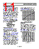
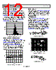
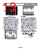
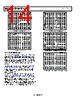
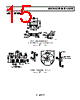
12 / 16 page  AD1582/AD1583/AD1584/AD1585 Data Sheet Rev. J | Page 12 of 16 OUTPUT VOLTAGE HYSTERESIS High performance industrial equipment manufacturers can require the AD1582/AD1583/AD1584/AD1585 to maintain a consistent output voltage error at 25°C after the references are operated over the full temperature range. All references exhibit a characteristic known as output voltage hysteresis; however, the AD1582/AD1583/AD1584/AD1585 are designed to minimize this characteristic. This phenomenon can be quantified by mea- suring the change in the +25°C output voltage after temperature excursions from +125°C to +25°C and from −40°C to +25°C. Figure 13 displays the distribution of the AD1582/AD1583/ AD1584/AD1585 output voltage hysteresis. 80 70 60 50 –700 –450 –200 50 300 550 40 30 20 10 0 ppm Figure 13. Output Voltage Hysteresis Distribution SUPPLY CURRENT VS. TEMPERATURE The quiescent current for the AD1582/AD1583/AD1584/ AD1585 varies slightly over temperature and input supply range. Figure 14 illustrates the typical performance for the AD1582/AD1583/AD1584/AD1585 reference when varying both temperature and supply voltage. As is evident from Figure 14, the AD1582/AD1583/AD1584/AD1585 supply current increases only 1.0 μA/V, making this device extremely attractive for use in applications where there can be wide variations in supply voltage and a need to minimize power dissipation. 100 80 60 40 20 0 VIN (V) 34 5 6 7 8 9 10 11 TA = +25°C TA = +85°C TA = –40°C Figure 14. Typical Supply Current over Temperature SUPPLY VOLTAGE One of the ideal features of the AD1582/AD1583/AD1584/AD1585 is low supply voltage headroom. The parts can operate at supply voltages as low as 200 mV above VOUT and up to 12 V. However, if negative voltage is inadvertently applied to VIN with respect to ground, or any negative transient >5 V is coupled to VIN, the device can be damaged. AC PERFORMANCE To apply the AD1582/AD1583/AD1584/AD1585, it is important to understand the effects of dynamic output impedance and power supply rejection. In Figure 15, a voltage divider is formed by the AD1582/AD1583/AD1584/ AD1585 output impedance and by the external source impedance. Figure 16 shows the effect of varying the load capacitor on the reference output. Power supply rejection ratio (PSRR) should be determined when characterizing the ac performance of a series voltage reference. Figure 17 shows a test circuit used to measure PSRR, and Figure 18 demonstrates the ability of the AD1582/AD1583/ AD1584/AD1585 to attenuate line voltage ripple. 5V 5µF 1µF 2×VOUT 10kΩ 10kΩ 2kΩ 10kΩ ±2V ±100µA ×1 VLOAD DC DUT Figure 15. Output Impedance Test Circuit 100 AD1585 AD1582 10 1 0.1 10 100 1k 10k 100k 1M FREQUENCY (Hz) 1µF CAP Figure 16. Output Impedance vs. Frequency 5V ± 100mV 0.22µF 0.22µF 10V 10kΩ 10kΩ ±200mV ×1 DUT VOUT Figure 17. Ripple Rejection Test Circuit |
|
|
链接网址 |
| ALLDATASHEET是否为您带来帮助? [ DONATE ] |
关于 Alldatasheet | 广告服务 | 联系我们 | 隐私政策 | 数据表链接 | 链接交换 | 制造商名单 All Rights Reserved©Alldatasheet.com |
| Russian : Alldatasheetru.com | Korean : Alldatasheet.co.kr | Spanish : Alldatasheet.es | French : Alldatasheet.fr | Italian : Alldatasheetit.com Portuguese : Alldatasheetpt.com | Polish : Alldatasheet.pl | Vietnamese : Alldatasheet.vn Indian : Alldatasheet.in | Mexican : Alldatasheet.com.mx | British : Alldatasheet.co.uk | New Zealand : Alldatasheet.co.nz |
|
Family Site : ic2ic.com |
icmetro.com |
 Chinese ▼
 English
 Chinese
 German
 Japanese
 Russian
 Korean
 Spanish
 French
 Italian
 Portuguese
 Polish
 Vietnamese
 Indian
 Mexican
 British
 New Zealand