|
数据搜索系统,热门电子元器件搜索 |
|
|
数据搜索系统,热门电子元器件搜索 |
|
AD1583ARTZ-R2 数据表(PDF) 11 Page - Analog Devices |
|
|
|||||||||||||||||||||||||||||
AD1583ARTZ-R2 数据表(HTML) 11 Page - Analog Devices |
|
|
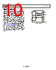
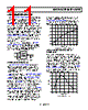
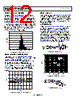
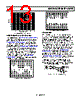
11 / 16 page  Data Sheet AD1582/AD1583/AD1584/AD1585 Rev. J | Page 11 of 16 APPLICATIONS INFORMATION The AD1582/AD1583/AD1584/AD1585 are series references that can be used for many applications. To achieve optimum performance with these references, only two external compo- nents are required. Figure 10 shows the AD1582/AD1583/ AD1584/AD1585 configured for operation under all loading conditions. With a simple 4.7 µF capacitor attached to the input and a 1 µF capacitor applied to the output, the devices can achieve specified performance for all input voltage and output current requirements. For best transient response, add a 0.1 µF capacitor in parallel with the 4.7 µF capacitor. While a 1 µF output capacitor can provide stable performance for all loading conditions, the AD1582/AD1583/AD1584/AD1585 can operate under low (−100 µA < IOUT < +100 µA) current conditions with just a 0.2 µF output capacitor. The 4.7 µF capacitor on the input can be reduced to 1 μF in this condition. Unlike conventional shunt reference designs, the AD1582/ AD1583/AD1584/AD1585 provide stable output voltages at constant operating current levels. When properly decoupled, as shown in Figure 10, these devices can be applied to any circuit and provide superior low power solutions. VOUT 1 2 VIN 3 AD1582/ AD1583/ AD1584/ AD1585 1µF 4.7µF + – Figure 10. Typical Connection Diagram TEMPERATURE PERFORMANCE The AD1582/AD1583/AD1584/AD1585 are designed for applications where temperature performance is important. Extensive temperature testing and characterization ensure that device performance is maintained over the specified temperature range. The error band guaranteed with the AD1582/AD1583/AD1584/ AD1585 is the maximum deviation from the initial value at 25°C. Therefore, for a given grade of the AD1582/AD1583/AD1584/ AD1585, the designer can easily determine the maximum total error by summing initial accuracy and temperature variation. For example, for the AD1582BRT, the initial tolerance is ±2 mV, and the temperature error band is ±8 mV; therefore, the reference is guaranteed to be 2.5 V ± 10 mV from −40°C to +125°C. Figure 11 shows the typical output voltage drift for the AD1582/ AD1583/AD1584/AD1585 and illustrates the methodology. The box in Figure 11 is bounded on the x-axis by operating tempera- ture extremes. It is bounded on the y-axis by the maximum and minimum output voltages observed over the operating temperature range. The slope of the diagonal drawn from the initial output value at 25°C to the output values at +125°C and −40°C determines the performance grade of the device. Duplication of these results requires a test system that is highly accurate with stable temperature control. Evaluation of the AD1582/AD1583/AD1584/AD1585 produces curves similar to those in Figure 5 and Figure 11, but output readings can vary depending on the test methods and test equipment used. 2.504 2.502 2.500 2.498 2.496 2.494 2.492 TEMPERATURE (°C) –40 –20 0 20 40 60 80 100 120 2.504 2.502 2.500 2.498 2.496 2.494 2.492 TEMPERATURE (°C) –40 –20 0 20 40 60 80 100 120 Figure 11. Output Voltage vs. Temperature VOLTAGE OUTPUT NONLINEARITY VS. TEMPERATURE When using a voltage reference with data converters, it is important to understand the impact that temperature drift can have on converter performance. The nonlinearity of the reference output drift represents additional error that cannot be easily calibrated out of the overall system. To better understand the impact such a drift can have on a data converter, refer to Figure 12, where the measured drift characteristic is normalized to the endpoint average drift. The residual drift error for the AD1582/ AD1583/AD1584/AD1585 of approximately 200 ppm demon- strates that these parts are compatible with systems that require 12-bit accurate temperature performance. 250 200 150 100 50 0 –50 TEMPERATURE (°C) –50 –25 0 25 50 75 100 Figure 12. Residual Drift Error |
|
|
链接网址 |
| ALLDATASHEET是否为您带来帮助? [ DONATE ] |
关于 Alldatasheet | 广告服务 | 联系我们 | 隐私政策 | 数据表链接 | 链接交换 | 制造商名单 All Rights Reserved©Alldatasheet.com |
| Russian : Alldatasheetru.com | Korean : Alldatasheet.co.kr | Spanish : Alldatasheet.es | French : Alldatasheet.fr | Italian : Alldatasheetit.com Portuguese : Alldatasheetpt.com | Polish : Alldatasheet.pl | Vietnamese : Alldatasheet.vn Indian : Alldatasheet.in | Mexican : Alldatasheet.com.mx | British : Alldatasheet.co.uk | New Zealand : Alldatasheet.co.nz |
|
Family Site : ic2ic.com |
icmetro.com |
 Chinese ▼
 English
 Chinese
 German
 Japanese
 Russian
 Korean
 Spanish
 French
 Italian
 Portuguese
 Polish
 Vietnamese
 Indian
 Mexican
 British
 New Zealand