|
数据搜索系统,热门电子元器件搜索 |
|
|
数据搜索系统,热门电子元器件搜索 |
|
ADG904-R 数据表(PDF) 1 Page - Analog Devices |
|
|
|||||||||||||||||||||||||||||
ADG904-R 数据表(HTML) 1 Page - Analog Devices |
|
|
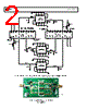
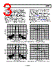
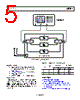
1 / 6 page  Circuit Note CN-0211 Circuits from the Lab™ reference circuits are engineered and testedfor quickandeasysystemintegrationtohelpsolvetoday’s analog, mixed-signal, and RF design challenges. For more informationand/orsupport, visitwww.analog.com/CN0211. Devices Connected/Referenced ADG904-R Wideband 2.5 GHz, 37 dB Isolation at 1 GHz, CMOS, 1.65 V to 2.75 V, 4:1 Mux/SP4T IF Band-Pass Filter Bank Switching Network for Wireless Infrastructure Rev.0 CircuitsfromtheLab™circuitsfromAnalogDeviceshavebeendesignedandbuiltbyAnalogDevices engineers. Standard engineering practices have been employed in the design and construction of eachcircuit,andtheirfunctionandperformancehavebeentestedandverifiedinalabenvironmentat room temperature. However, you are solely responsible for testing the circuit and determining its suitabilityandapplicabilityforyouruseandapplication.Accordingly,innoeventshallAnalogDevices be liable for direct, indirect, special, incidental, consequential or punitive damages due to any cause whatsoeverconnectedtotheuseofanyCircuitsfromtheLabcircuits. (Continuedonlastpage) One Technology Way, P.O. Box 9106, Norwood, MA 02062-9106, U.S.A. Tel: 781.329.4700 www.analog.com Fax: 781.461.3113 ©2011 Analog Devices, Inc. All rights reserved. EVALUATION AND DESIGN SUPPORT Circuit Evaluation Boards CN-0211 Circuit Evaluation Board (EVAL-CN0211-EB1Z) Design and Integration Files Schematics, Layout Files, Bill of Materials CIRCUIT FUNCTION AND BENEFITS The function of the circuit, shown in Figure 1, is to route an RF signal through an IF band-pass filter bank. The circuit uses three 140 MHz IF SAW filters with different bandwidths and two ADG904-R SP4T CMOS RF switches. The ADG904-R switches control which band-pass filter the RF signal will pass through. Only one filter is selectable at a time. The typical name given to this type of switching is “filter bank switching.” This application is very common in wireless infrastructure applications, such as cell phone base stations and point-to- point radio RF front ends. Selecting IF filters with different bandwidths results in more flexibility in controlling the various data rates in these systems. Insertion loss versus frequency in the IF band must be flat to achieve optimum system performance. The ADG904-R switch is ideally suited for this circuit because it has very flat insertion loss versus frequency. The insertion loss also remains flat over the supply voltage and temperature range. Switch off isolation is another very important parameter to maximize the performance of this circuit. The ADG904-R has excellent off isolation of greater than −50 dB up to 200 MHz. CIRCUIT DESCRIPTION The circuit consists of two ADG904-R CMOS RF switches and three IF SAW filters connected as shown in Figure 1. The switches have a supply voltage range of 1.65 V to 2.75 V. In this evaluation, a nominal value of 2.5 V is used. The RF input is connected to Pin 10 (RFC) of the ADG904-R switch, U1. The ADG904-R switch is a SP4T switch where the RFC pin is the common connection to all four switches (RF1, RF2, RF3 and RF4). Pin 4 of U1 (RF1) is connected to the input of the Triquint 856592 SAW filter. This filter is a single ended filter with a characteristic impedance of 50 Ω. It has a center frequency of 140 MHz and a typical 1 dB bandwidth of 20.7 MHz. Note that lumped element matching is required to achieve the optimum 50 Ω termination impedance. The output of the filter is connected to pin 17 (RF2) of the ADG904-R, U2. Similarly, the second SAW filter (Triquint 856684) is connected to U1 and U2. In this case, the filter is connected to Pin 17 (RF2) of U1 and Pin 4 (RF1) of U2. The 856684 filter has a center frequency of 140 MHz and a typical 1 dB bandwidth of 16.18 MHz. The third SAW filter (Triquint 856656) is connected to Pin 7 (RF3) of U1 and Pin 14 (RF4) of U2. The 856656 filter has a centre frequency of 140 MHz and a typical 1 dB bandwidth of 11.82 MHz It is important to use the PCB land layout pattern recommended by the manufacturer of the SAW filters. To achieve the maximum isolation from the input port to the output port, a plated slot was positioned under the filter. Improving this isolation enables the full out-of-band attenuation to be achieved and minimizes the in-band ripple. Each filter is matched to 50 Ω on the input port and output port using 0603 size inductor and capacitor lumped elements. This is an important aspect for achieving good performance from the circuit evaluation board. To further improve isolation, the 50 Ω transmission lines that connect the filters to the switches and to the RF edge connectors are designed as coplanar waveguides. The standalone insertion loss vs. frequency for the 11.82 MHz bandwidth filter is shown in Figure 3. This data was measured with the filter on a separate circuit evaluation PCB with the same transmission line design and matching components, but with no switches in the RF path. This response is used as reference data. The insertion loss at 140 MHz was −9.17 dB, which is consistent with the data sheet value of −9.2 dB typical. |
类似零件编号 - ADG904-R |
|
类似说明 - ADG904-R |
|
|
|
链接网址 |
| ALLDATASHEET是否为您带来帮助? [ DONATE ] |
关于 Alldatasheet | 广告服务 | 联系我们 | 隐私政策 | 数据表链接 | 链接交换 | 制造商名单 All Rights Reserved©Alldatasheet.com |
| Russian : Alldatasheetru.com | Korean : Alldatasheet.co.kr | Spanish : Alldatasheet.es | French : Alldatasheet.fr | Italian : Alldatasheetit.com Portuguese : Alldatasheetpt.com | Polish : Alldatasheet.pl | Vietnamese : Alldatasheet.vn Indian : Alldatasheet.in | Mexican : Alldatasheet.com.mx | British : Alldatasheet.co.uk | New Zealand : Alldatasheet.co.nz |
|
Family Site : ic2ic.com |
icmetro.com |
 Chinese ▼
 English
 Chinese
 German
 Japanese
 Russian
 Korean
 Spanish
 French
 Italian
 Portuguese
 Polish
 Vietnamese
 Indian
 Mexican
 British
 New Zealand