|
数据搜索系统,热门电子元器件搜索 |
|
|
数据搜索系统,热门电子元器件搜索 |
|
AD8652ARMZ-R2 数据表(PDF) 16 Page - Analog Devices |
|
|
|||||||||||||||||||||||||||||
AD8652ARMZ-R2 数据表(HTML) 16 Page - Analog Devices |
|
|
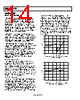
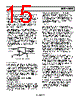
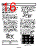
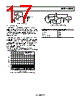
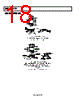
16 / 20 page  AD8651/AD8652 Rev. C | Page 16 of 20 Input Capacitance Along with bypassing and grounding, high speed amplifiers can be sensitive to parasitic capacitance between the inputs and ground. A few picofarads of capacitance reduces the input impedance at high frequencies, which in turn increases the amplifier gain, causing peaking in the frequency response or oscillations. With the AD865x, additional input damping is required for stability with capacitive loads greater than 47 pF with direct input to output feedback (see the Output Capacitance section). Output Capacitance When using high speed amplifiers, it is important to consider the effects of the capacitive loading on amplifier stability. Capacitive loading interacts with the output impedance of the amplifier, causing reduction of the BW as well as peaking and ringing of the frequency response. To reduce the effects of the capacitive loading and allow higher capacitive loads, there are two commonly used methods. • As shown in Figure 56, place a small value resistor (RS) in series with the output to isolate the load capacitor from the amplifier output. Heavy capacitive loads can reduce the phase margin of an amplifier and cause the amplifier response to peak or become unstable. The AD865x is able to drive up to 47 pF in a unity gain buffer configuration without oscillation or external compensation. However, if an application requires a higher capacitive load drive when the AD865x is in unity gain, the use of external isolation networks can be used. The effect produced by this resistor is to isolate the op amp output from the capacitive load. The required amount of series resistance has been tabulated in Table 5 for different capacitive loads. While this technique improves the overall capacitive load drive for the amplifier, its biggest drawback is that it reduces the output swing of the overall circuit. VIN 0 0 0 3 2 U1 RL CL RS VOUT VCC + – AD865x V+ V– Figure 56. Driving Large Capacitive Loads Table 5. Optimum Values for Driving Large Capacitive Loads CL RS 100 pF 50 Ω 500 pF 35 Ω 1.0 nF 25 Ω • Another way to stabilize an op amp driving a large capacitive load is to use a snubber network, as shown in Figure 57. Because there is not any isolation resistor in the signal path, this method has the significant advantage of not reducing the output swing. The exact values of RS and CS are derived experimentally. In Figure 57, an optimum RS and CS combination for a capacitive load drive ranging from 50 pF to 1 nF was chosen. For this, RS = 3 Ω and CS = 10 nF were chosen. 200mV RL CL RS CS VOUT V+ V– + – AD865x V+ V– Figure 57. Snubber Network Settling Time The settling time of an amplifier is defined as the time it takes for the output to respond to a step change of input and enter and remain within a defined error band, as measured relative to the 50% point of the input pulse. This parameter is especially important in measurements and control circuits where amplifi- ers are used to buffer A/D inputs or DAC outputs. The design of the AD865x family combines a high slew rate and a wide gain bandwidth product to produce an amplifier with very fast settling time. The AD865x is configured in the noninverting gain of 1 with a 2 V p-p step applied to its input. The AD865x family has a settling time of about 130 ns to 0.01% (2 mV). The output is monitored with a 10×, 10 M, 11.2 pF scope probe. THD Readings vs. Common-Mode Voltage Total harmonic distortion of the AD865x family is well below 0.0004% with any load down to 600 Ω. The distortion is a function of the circuit configuration, the voltage applied, and the layout, in addition to other factors. The AD865x family outperforms its competitor for distortion, especially at frequencies below 20 kHz, as shown in Figure 58. 0.0001 0.0002 0.0005 0.001 0.002 0.005 0.01 0.02 0.05 0.1 FREQUENCY (Hz) VSY = +3.5V/–1.5V VOUT = 2.0V p-p 20 50 100 500 20k 5k 2k 1k OPA350 AD8651 Figure 58. Total Harmonic Distortion |
|
|
链接网址 |
| ALLDATASHEET是否为您带来帮助? [ DONATE ] |
关于 Alldatasheet | 广告服务 | 联系我们 | 隐私政策 | 数据表链接 | 链接交换 | 制造商名单 All Rights Reserved©Alldatasheet.com |
| Russian : Alldatasheetru.com | Korean : Alldatasheet.co.kr | Spanish : Alldatasheet.es | French : Alldatasheet.fr | Italian : Alldatasheetit.com Portuguese : Alldatasheetpt.com | Polish : Alldatasheet.pl | Vietnamese : Alldatasheet.vn Indian : Alldatasheet.in | Mexican : Alldatasheet.com.mx | British : Alldatasheet.co.uk | New Zealand : Alldatasheet.co.nz |
|
Family Site : ic2ic.com |
icmetro.com |
 Chinese ▼
 English
 Chinese
 German
 Japanese
 Russian
 Korean
 Spanish
 French
 Italian
 Portuguese
 Polish
 Vietnamese
 Indian
 Mexican
 British
 New Zealand