|
数据搜索系统,热门电子元器件搜索 |
|
|
数据搜索系统,热门电子元器件搜索 |
|
AD8051ART-R2 数据表(PDF) 17 Page - Analog Devices |
|
|
|||||||||||||||||||||||||||||
AD8051ART-R2 数据表(HTML) 17 Page - Analog Devices |
|
|
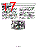
17 / 25 page  AD8051/AD8052/AD8054 Rev. J | Page 16 of 24 THEORY OF OPERATION CIRCUIT DESCRIPTION The AD8051/AD8052/AD8054 are fabricated on the Analog Devices, Inc. proprietary eXtra-Fast Complementary Bipolar (XFCB) process, which enables the construction of PNP and NPN transistors with similar fTs in the 2 GHz to 4 GHz region. The process is dielectrically isolated to eliminate the parasitic and latch-up problems caused by junction isolation. These features allow the construction of high frequency, low distortion amplifiers with low supply currents. This design uses a differential output input stage to maximize bandwidth and headroom (see Figure 40). The smaller signal swings required on the first stage outputs (nodes SIP, SIN) reduce the effect of nonlinear currents due to junction capacitances and improve the distortion per- formance. This design achieves harmonic distortion of −80 dBc @ 1 MHz into 100 Ω with VOUT = 2 V p-p (gain = +1) on a single 5 V supply. The inputs of the device can handle voltages from −0.2 V below the negative rail to within 1 V of the positive rail. Exceeding these values do not cause phase reversal; however, the input ESD devices begin to conduct if the input voltages exceed the rails by greater than 0.5 V. During this overdrive condition, the output stays at the rail. The rail-to-rail output range of the AD8051/AD8052/AD8054 is provided by a complementary common emitter output stage. High output drive capability is provided by injecting all output stage predriver currents directly into the bases of the output devices Q8 and Q36. Biasing of Q8 and Q36 is accomplished by I8 and I5, along with a common-mode feedback loop (not shown). This circuit topology allows the AD8051/AD8052 to drive 45 mA of output current and allows the AD8054 to drive 30 mA of output current with the outputs within 0.5 V of the supply rails. I10 R39 VEE I2 I3 Q25 Q51 R23 R27 I9 Q36 I5 VEE C3 C9 I8 VCC I11 I7 R3 R21 R5 Q3 SIP SIN C7 Q4 R15 R2 R26 Q50 Q22 Q21 Q27 Q7 Q8 Q23 Q31 Q39 Q13 Q1 Q24 Q47 Q11 Q2 Q5 Q40 VOUT VCC VINP VINN VEE Figure 40. AD8051/AD8052 Simplified Schematic |
|
|
链接网址 |
| ALLDATASHEET是否为您带来帮助? [ DONATE ] |
关于 Alldatasheet | 广告服务 | 联系我们 | 隐私政策 | 数据表链接 | 链接交换 | 制造商名单 All Rights Reserved©Alldatasheet.com |
| Russian : Alldatasheetru.com | Korean : Alldatasheet.co.kr | Spanish : Alldatasheet.es | French : Alldatasheet.fr | Italian : Alldatasheetit.com Portuguese : Alldatasheetpt.com | Polish : Alldatasheet.pl | Vietnamese : Alldatasheet.vn Indian : Alldatasheet.in | Mexican : Alldatasheet.com.mx | British : Alldatasheet.co.uk | New Zealand : Alldatasheet.co.nz |
|
Family Site : ic2ic.com |
icmetro.com |
 Chinese ▼
 English
 Chinese
 German
 Japanese
 Russian
 Korean
 Spanish
 French
 Italian
 Portuguese
 Polish
 Vietnamese
 Indian
 Mexican
 British
 New Zealand