|
数据搜索系统,热门电子元器件搜索 |
|
|
数据搜索系统,热门电子元器件搜索 |
|
AD8057ART-R2 数据表(PDF) 15 Page - Analog Devices |
|
|
|||||||||||||||||||||||||||||
AD8057ART-R2 数据表(HTML) 15 Page - Analog Devices |
|
|
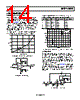
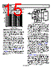
15 / 17 page  AD8057/AD8058 Data Sheet Rev. D | Page 14 of 16 Figure 47 shows a frequency sweep of this filter. The response is down 3 dB at 5.7 MHz; therefore, it passes the video band with little attenuation. The rejection at 27 MHz is 42 dB, which provides more than a factor of 100 in suppression of the clock components at this frequency. FREQUENCY (MHz) 0 10 –10 –90 –70 –80 –60 100k 100M 10M 1M –20 –30 –50 –40 Figure 47. Video Filter Response DIFFERENTIAL ANALOG-TO-DIGITAL DRIVER As system supply voltages are dropping, many ADCs provide differential analog inputs to increase the dynamic range of the input signal while still operating on a low supply voltage. Differential driving can also reduce second and other even- order distortion products. Analog Devices, Inc., offers an assortment of 12- and 14-bit high speed converters that have differential inputs and can be run from a single 5 V supply. These include the AD9220, AD9221, AD9223, AD9224, and AD9225 at 12 bits, and the AD9240, AD9241, and AD9243 at 14 bits. Although these devices can operate over a range of common-mode voltages at their analog inputs, they work best when the common-mode voltage at the input is at the midsupply or 2.5 V. Op amp architectures that require upwards of 2 V of headroom at the output have significant problems when trying to drive such ADCs while operating with a 5 V positive supply. The low headroom output design of the AD8057 and AD8058 make them ideal for driving these types of ADCs. The AD8058 can be used to make a dc-coupled, single-ended- to-differential driver for one of these ADCs. Figure 48 is a schematic of such a circuit for driving an AD9225, 12-bit, 25 MSPS ADC. 2 3 0.1µF 10µF 0.1µF 10µF 0.1µF 10µF + 8 1 +5V 1kΩ AD8058 1kΩ 1kΩ 1kΩ 1kΩ 50Ω 50Ω 1kΩ 1kΩ 1kΩ 6 5 7 + –5V 4 VIN 0V VINB VINA AD9225 +5V + REF +2.5V AD8058 Figure 48. Schematic Circuit for Driving AD9225 In this circuit, one of the op amps is configured in the inverting mode whereas the other is in the noninverting mode. However, to provide better bandwidth matching, each op amp is configured for a noise gain of +2. The inverting op amp is configured for a gain of −1 and the noninverting op amp is configured for a gain of +2. Each of these produces a noise gain of +2, which is deter- mined only by the inverse of the feedback ratio. The input signal to the noninverting op amp is divided by two to normalize its level and make it equal to the inverting output. For 0 V input, the outputs of the op amps want to be at 2.5 V, which is the midsupply level of the ADCs. This is accomplished by first taking the 2.5 V reference output of the ADC and dividing it by two by a pair of 1 kΩ resistors. The resulting 1.25 V is applied to the positive input of each op amp. This voltage is then multiplied by the gain of +2 of the op amps to provide a 2.5 V level at each output. The assumption for this circuit is that the input signal is bipolar with respect to ground and the circuit must be dc-coupled thereby implying the existence of a negative supply elsewhere in the system. This circuit uses −5 V as the negative supply for the AD8058. Tying the negative supply of the AD8058 to ground causes a problem at the input of the noninverting op amp. The input common-mode voltage can only go to within 1 V of the negative rail. Because this circuit requires that the positive inputs operate with a 1.25 V bias, there is not enough room to swing this voltage in the negative direction. The inverting stage does not have this problem because its common-mode input voltage remains fixed at 1.25 V. If dc coupling is not required, various ac coupling techniques can be used to eliminate this problem. LAYOUT The AD8057 and AD8058 are high speed op amps for use in a board layout that follows standard high speed design rules. Make all signal traces as short and direct as possible. In particular, keep the parasitic capacitance on the inverting input of each device to a minimum to avoid excessive peaking and other undesirable performance. Bypass the power supplies very close to the power pins of the package with a 0.1 µF capacitor in parallel with a larger (approximately 10 µF) tantalum capacitor. Connect these capacitors to a ground plane that either is on an inner layer or fills the area of the board that is not used for other signals. |
|
|
链接网址 |
| ALLDATASHEET是否为您带来帮助? [ DONATE ] |
关于 Alldatasheet | 广告服务 | 联系我们 | 隐私政策 | 数据表链接 | 链接交换 | 制造商名单 All Rights Reserved©Alldatasheet.com |
| Russian : Alldatasheetru.com | Korean : Alldatasheet.co.kr | Spanish : Alldatasheet.es | French : Alldatasheet.fr | Italian : Alldatasheetit.com Portuguese : Alldatasheetpt.com | Polish : Alldatasheet.pl | Vietnamese : Alldatasheet.vn Indian : Alldatasheet.in | Mexican : Alldatasheet.com.mx | British : Alldatasheet.co.uk | New Zealand : Alldatasheet.co.nz |
|
Family Site : ic2ic.com |
icmetro.com |
 Chinese ▼
 English
 Chinese
 German
 Japanese
 Russian
 Korean
 Spanish
 French
 Italian
 Portuguese
 Polish
 Vietnamese
 Indian
 Mexican
 British
 New Zealand