|
数据搜索系统,热门电子元器件搜索 |
|
|
数据搜索系统,热门电子元器件搜索 |
|
AD8232ACPZ-R7 数据表(PDF) 21 Page - Analog Devices |
|
|
|||||||||||||||||||||||||||||
AD8232ACPZ-R7 数据表(HTML) 21 Page - Analog Devices |
|
|
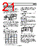
21 / 28 page  Data Sheet AD8232 Rev. A | Page 21 of 28 APPLICATIONS INFORMATION ELIMINATING ELECTRODE OFFSETS The instrumentation amplifier in the AD8232 is designed to apply gain and to filter out near dc signals simultaneously. This capability allows it to amplify a small ECG signal by a factor of 100 yet reject electrode offsets as large as ±300 mV. To achieve offset rejection, connect an RC network between the output of the instrumentation amplifier, HPSENSE, and HPDRIVE, as shown in Figure 53. Figure 53. Eliminating Electrode Offsets This RC network forms an integrator that feeds any near dc signals back into the instrumentation amplifier, thus eliminating the offsets without saturating any node and maintaining high signal gain. In addition to blocking offsets present across the inputs of the instrumentation amplifier, this integrator also works as a high- pass filter that minimizes the effect of slow moving signals, such as baseline wander. The cutoff frequency of the filter is given by the equation RC f dB 2 100 3 where R is in ohms and C is in farads. Note that the filter cutoff is 100 times higher than is typically expected from a single-pole filter. Because of the feedback architecture of the instrumentation amplifier, the typical filter cutoff equation is modified by the gain of 100 of the instrumentation amplifier. Figure 54. Frequency Response of Single-Pole DC Blocking Circuit Just like with any high-pass filter with low frequency cutoff, any fast change in dc offset takes a long time to settle. If such change saturates the instrumentation amplifier output, the S1 switch briefly enables the 10 kΩ resistor path, thus moving the cutoff frequency to ) 10 ( 2 ) 10 ( 100 4 4 3 RC R f dB (1) For values of R greater than 100 kΩ, the expression in Equation 1 can be approximated by C f dB 200 1 3 This higher cutoff reduces the settling time and enables faster recovery of the ECG signal. For more information, see the Fast Restore Circuit section. HIGH-PASS FILTERING The AD8232 can implement higher order high-pass filters. A higher filter order yields better artifact rejection but at a cost of increased signal distortion and more passive components on the printed circuit board (PCB). Two-Pole High-Pass Filter A two-pole architecture can be implemented by adding a simple ac coupling RC at the output of the instrumentation amplifier, as shown in Figure 55. Figure 55. Schematic for a Two-Pole High-Pass Filter Note that the right side of C2 connects to the SW terminal. Just like S1, S2 reduces the recovery time for this ac coupling network by placing 10 kΩ in parallel with R2. See the Fast Restore Circuit section for additional details on switch timing and trigger conditions. Keep in mind that if this passive network is not buffered, it exhibits higher output impedance at the input of a subsequent low-pass filter, such as with Sallen-Key filter topologies. Careful component selection can yield good results without a buffer. See the Low-Pass Filtering and Gain section for additional information on component selection. 10kΩ IAOUT HPSENSE HPDRIVE S1 GM1 GM2 99R R IN+ IN– VCM H PA ELECTRODE OFFSETS C R = REFOUT 19 3 1 20 2 C1 50 40 10 20 30 0 0.01 100 10 1 0.1 FREQUENCY (Hz) 20dB PER DECADE 10kΩ IAOUT HPSENSE HPDRIVE S1 +IN –IN HPA SW 10kΩ S2 6 REFOUT 8 TO NEXT STAGE = REFOUT 19 3 1 20 2 C1 C2 R1 R2 |
|
|
链接网址 |
| ALLDATASHEET是否为您带来帮助? [ DONATE ] |
关于 Alldatasheet | 广告服务 | 联系我们 | 隐私政策 | 数据表链接 | 链接交换 | 制造商名单 All Rights Reserved©Alldatasheet.com |
| Russian : Alldatasheetru.com | Korean : Alldatasheet.co.kr | Spanish : Alldatasheet.es | French : Alldatasheet.fr | Italian : Alldatasheetit.com Portuguese : Alldatasheetpt.com | Polish : Alldatasheet.pl | Vietnamese : Alldatasheet.vn Indian : Alldatasheet.in | Mexican : Alldatasheet.com.mx | British : Alldatasheet.co.uk | New Zealand : Alldatasheet.co.nz |
|
Family Site : ic2ic.com |
icmetro.com |
 Chinese ▼
 English
 Chinese
 German
 Japanese
 Russian
 Korean
 Spanish
 French
 Italian
 Portuguese
 Polish
 Vietnamese
 Indian
 Mexican
 British
 New Zealand