|
数据搜索系统,热门电子元器件搜索 |
|
|
数据搜索系统,热门电子元器件搜索 |
|
ADR381ARTZ-R2 数据表(PDF) 12 Page - Analog Devices |
|
|
|||||||||||||||||||||||||||||
ADR381ARTZ-R2 数据表(HTML) 12 Page - Analog Devices |
|
|
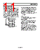
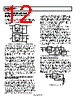
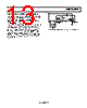
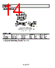
12 / 16 page  ADR380/ADR381 Rev. C | Page 12 of 16 APPLICATIONS INFORMATION STACKING REFERENCE ICs FOR ARBITRARY OUTPUTS Some applications may require two reference voltage sources, which are a combined sum of standard outputs. The following circuit shows how this stacked output reference can be implemented: GND VOUT VIN 3 GND VOUT VIN C2 1µF C1 0.1µF C3 0.1µF C4 1µF 3 R1 3.9k Ω VOUT2 VOUT1 2 2 1 1 VIN U2 ADR380/ ADR381 U1 ADR380/ ADR381 Figure 27. Stacking Voltage References with the ADR380/ADR381 Two ADR380s or ADR381s are used; the outputs of the individ- ual references are simply cascaded to reduce the supply current. Such configuration provides two output voltages: VOUT1 and VOUT2. VOUT1 is the terminal voltage of U1, while VOUT2 is the sum of this voltage and the terminal voltage of U2. U1 and U2 can be chosen for the two different voltages that supply the required outputs. While this concept is simple, a precaution is in order. Because the lower reference circuit must sink a small bias current from U2, plus the base current from the series PNP output transistor in U2, the external load of either U1 or R1 must provide a path for this current. If the U1 minimum load is not well-defined, Resistor R1 should be used, set to a value that conservatively passes 600 μA of current with the applicable VOUT1 across it. Note that the two U1 and U2 reference circuits are locally treated as macrocells, each having its own bypasses at input and output for optimum stability. Both U1 and U2 in this circuit can source dc currents up to their full rating. The minimum input voltage, VIN, is determined by the sum of the outputs, VOUT2, plus the 300 mV dropout voltage of U2. A NEGATIVE PRECISION REFERENCE WITHOUT PRECISION RESISTORS In many current-output CMOS DAC applications where the output signal voltage must be of the same polarity as the reference voltage, it is often required to reconfigure a current- switching DAC into a voltage-switching DAC through the use of a 1.25 V reference, an op amp, and a pair of resistors. Using a current switching DAC directly requires an additional opera- tional amplifier at the output to reinvert the signal. A negative voltage reference is then desirable from the point that an additional operational amplifier is not required for either reinversion (current-switching mode) or amplification (voltage-switching mode) of the DAC output voltage. In general, any positive voltage reference can be converted into a negative voltage reference through the use of an operational amplifier and a pair of matched resistors in an inverting configuration. The disadvantage to this approach is that the largest single source of error in the circuit is the relative matching of the resistors used. The circuit in Figure 28 avoids the need for tightly matched resistors with the use of an active integrator circuit. In this circuit, the output of the voltage reference provides the input drive for the integrator. The integrator, to maintain circuit equilibrium, adjusts its output to establish the proper relation- ship between the reference VOUT and GND. Thus, any negative output voltage desired can be chosen by substituting for the appropriate reference IC. A precaution should be noted with this approach: although rail-to-rail output amplifiers work best in the application, these operational amplifiers require a finite amount (mV) of headroom when required to provide any load current. The choice for the circuit’s negative supply should take this issue into account. GND VOUT VIN C2 0.1µF 3 +5V –VREF VIN 2 A1 1 U2 –5V OP195 –V +V C1 1µF U1 ADR380/ ADR381 R4 1k Ω R3 100k Ω C3 1µF C4 1µF R5 100 Ω Figure 28. Negative Precision Voltage Reference Using No Precision Resistors PRECISION CURRENT SOURCE Many times in low power applications, the need arises for a precision current source that can operate on low supply voltages. As shown in Figure 29, the ADR380/ADR381 can be configured as a precision current source. The circuit configuration illustrated is a floating current source with a grounded load. The reference output voltage is bootstrapped across RSET (R1 + P1), which sets the output current into the load. With this configuration, circuit precision is maintained for load currents in the range from the reference supply current, typically 90 μA to approximately 5 mA. GND VOUT VIN 3 VIN 2 R1 1 RL P1 IOUT ISY ADJUST U1 ADR380/ ADR381 C3 1µF C1 1µF C2 0.1µF Figure 29. Precision Current Source |
|
|
链接网址 |
| ALLDATASHEET是否为您带来帮助? [ DONATE ] |
关于 Alldatasheet | 广告服务 | 联系我们 | 隐私政策 | 数据表链接 | 链接交换 | 制造商名单 All Rights Reserved©Alldatasheet.com |
| Russian : Alldatasheetru.com | Korean : Alldatasheet.co.kr | Spanish : Alldatasheet.es | French : Alldatasheet.fr | Italian : Alldatasheetit.com Portuguese : Alldatasheetpt.com | Polish : Alldatasheet.pl | Vietnamese : Alldatasheet.vn Indian : Alldatasheet.in | Mexican : Alldatasheet.com.mx | British : Alldatasheet.co.uk | New Zealand : Alldatasheet.co.nz |
|
Family Site : ic2ic.com |
icmetro.com |
 Chinese ▼
 English
 Chinese
 German
 Japanese
 Russian
 Korean
 Spanish
 French
 Italian
 Portuguese
 Polish
 Vietnamese
 Indian
 Mexican
 British
 New Zealand