|
数据搜索系统,热门电子元器件搜索 |
|
|
数据搜索系统,热门电子元器件搜索 |
|
LTC1663 数据表(PDF) 8 Page - Linear Technology |
|
|
|||||||||||||||||||||||||||||
LTC1663 数据表(HTML) 8 Page - Linear Technology |
|
|
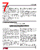
8 / 12 page  LTC1663 8 1663fd APPLICATIONS INFORMATION Bit (Wr) = 0. The LTC1663 acknowledges and the master delivers the command byte. The LTC1663 acknowledges and latches the command byte into the command byte input register. The master then delivers the least significant data byte. Again the LTC1663 acknowledges and the data is latched into the least significant data byte input register. The master then delivers the most significant data byte. The LTC1663 acknowledges once more and latches the data into the most significant data byte input register. Lastly, the master terminates the communication with a STOP condition. On the reception of the STOP condition, the LTC1663 transfers the input register information to output registers and the DAC output is updated. Slave Address (MSOP Package Only) The LTC1663 can respond to one of eight 7-bit addresses. The first 4 bits (MSBs) have been factory programmed to 0100. The first 4 bits of the LTC1663-8 have been factory programmed to 0011. The three address bits, AD2, AD1 and AD0 are programmed by the user and determine the LSBs of the slave address, as shown in the table below: LTC1663 LTC1663-8 AD2 AD1 AD0 0100 xxx 0011 xxx L L L 0100 000 0011 000 L L H 0100 001 0011 001 L H L 0100 010 0011 010 L H H 0100 011 0011 011 H L L 0100 100 0011 100 H L H 0100 101 0011 101 H H L 0100 110 0011 110 H H H 0100 111 0011 111 Slave Address (SOT-23 Package) The slave address for the SOT-23 package has been factory programmed to be “0100 000” (LTC1663), “0100 001” (LTC1663-1) and “0100 010” (LTC1663-2) If another address is required, please consult the factory. Command Byte 7 6543 2 1 0 X XXXX BG SD SY SY 1 0 Allows update on Acknowledge of SYNC Address only Update on Stop condition only (Power-On Default) SD 1 0 Puts the device in power-down mode Puts the device in standard operating mode (Power-On Default) BG 1 0 Selects the internal bandgap reference Selects the supply as the reference (Power-On Default) X X Don’t Care The stop condition normally initiates the update of the DAC’s output latches. Simultaneous update of more than one DAC or other devices on the bus can be achieved by reissuing new start bit, address, command and data bytes before issuing a final stop condition (which will update all the devices). An alternate way to achieve simultaneous LTC1663 updates is to override the stop condition update by setting the “SY” bit of the command byte. Setting this bit sets the device to update the DAC output latches only at the reception of a SYNC address quick command. The actual update occurs on the rising edge of SCL during the Acknowledge. In this way, all devices can update on the reception of the SYNC address quick command instead of the STOP condition. A Shutdown (SD) bit = HIGH will put the device in a low power state but retain all data latch information. Shutdown will occur at the reception of a STOP condition. This way shutdown could be synchronized to other devices. The output impedance of the DAC will go to a high impedance state (≈ 500kΩ to GND). The Bandgap (BG) bit when set to “0” selects the DAC supply voltage as its voltage reference. The full-scale output of the DAC with this setting is equal to the supply voltage. When the BG bit is set to “1,” the internal bandgap reference (≈1.25V) is selected as the DAC’s reference. The full-scale output voltage for this setting is 2.5V. |
|
|
链接网址 |
| ALLDATASHEET是否为您带来帮助? [ DONATE ] |
关于 Alldatasheet | 广告服务 | 联系我们 | 隐私政策 | 数据表链接 | 链接交换 | 制造商名单 All Rights Reserved©Alldatasheet.com |
| Russian : Alldatasheetru.com | Korean : Alldatasheet.co.kr | Spanish : Alldatasheet.es | French : Alldatasheet.fr | Italian : Alldatasheetit.com Portuguese : Alldatasheetpt.com | Polish : Alldatasheet.pl | Vietnamese : Alldatasheet.vn Indian : Alldatasheet.in | Mexican : Alldatasheet.com.mx | British : Alldatasheet.co.uk | New Zealand : Alldatasheet.co.nz |
|
Family Site : ic2ic.com |
icmetro.com |
 Chinese ▼
 English
 Chinese
 German
 Japanese
 Russian
 Korean
 Spanish
 French
 Italian
 Portuguese
 Polish
 Vietnamese
 Indian
 Mexican
 British
 New Zealand