|
数据搜索系统,热门电子元器件搜索 |
|
|
数据搜索系统,热门电子元器件搜索 |
|
IR3553 数据表(PDF) 20 Page - International Rectifier |
|
|
|||||||||||||||||||||||||||||
IR3553 数据表(HTML) 20 Page - International Rectifier |
|
|
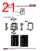
20 / 22 page  July 16, 2014 | DATASHEET V3.3 20 IR3553 40A Integrated PowIRstage® STENCIL DESIGN The stencil apertures for the lead lands should be approximately 65% to 75% of the area of the lead lands depending on stencil thickness. Reducing the amount of solder deposited will minimize the occurrence of lead shorts. Since for 0.5mm pitch devices the leads are only 0.25mm wide, the stencil apertures should not be made narrower; openings in stencils < 0.25mm wide are difficult to maintain repeatable solder release. The low power signal stencil lead land apertures should therefore be shortened in length to keep area ratio of 65% to 75% while centered on lead land. The power pads VIN, PGND, TGND and SW, land pad apertures should be approximately 65% to 75% area of solder on the center pad. If too much solder is deposited on the center pad the part will float and the lead lands will be open. Solder paste on large pads is broken down into small sections with a minimum gap of 0.2mm between allowing for out-gassing during solder reflow. The maximum length and width of the land pad stencil aperture should be equal to the solder resist opening minus an annular 0.2mm pull back to decrease the incidence of shorting the center land to the lead lands when the part is pushed into the solder paste. Figure 35: Stencil design * Contact International Rectifier to receive an electronic PCB Library file in Cadence Allegro or CAD DXF/DWG format. |
|
|
链接网址 |
| ALLDATASHEET是否为您带来帮助? [ DONATE ] |
关于 Alldatasheet | 广告服务 | 联系我们 | 隐私政策 | 数据表链接 | 链接交换 | 制造商名单 All Rights Reserved©Alldatasheet.com |
| Russian : Alldatasheetru.com | Korean : Alldatasheet.co.kr | Spanish : Alldatasheet.es | French : Alldatasheet.fr | Italian : Alldatasheetit.com Portuguese : Alldatasheetpt.com | Polish : Alldatasheet.pl | Vietnamese : Alldatasheet.vn Indian : Alldatasheet.in | Mexican : Alldatasheet.com.mx | British : Alldatasheet.co.uk | New Zealand : Alldatasheet.co.nz |
|
Family Site : ic2ic.com |
icmetro.com |
 Chinese ▼
 English
 Chinese
 German
 Japanese
 Russian
 Korean
 Spanish
 French
 Italian
 Portuguese
 Polish
 Vietnamese
 Indian
 Mexican
 British
 New Zealand