|
数据搜索系统,热门电子元器件搜索 |
|
|
数据搜索系统,热门电子元器件搜索 |
|
STP2CMP 数据表(PDF) 14 Page - STMicroelectronics |
|
|
|||||||||||||||||||||||||||||
STP2CMP 数据表(HTML) 14 Page - STMicroelectronics |
|
|
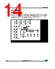
14 / 23 page  PCB layout STP2CMP 14/23 DocID022734 Rev 2 7 PCB layout 7.1 Recommended The STP2CMP is a charge pump power device so it requires a proper PCB layout in order to obtain the necessary stability and optimize line/load regulation and output voltage ripple. Input, output, and boost capacitors must be as close as possible to their relative pins.The example of the evaluation board below is shared with the STP4CMP device which is a pin compatible device with 4 current sources and the same architecture. Figure 9: Top layer |
|
|
链接网址 |
| ALLDATASHEET是否为您带来帮助? [ DONATE ] |
关于 Alldatasheet | 广告服务 | 联系我们 | 隐私政策 | 数据表链接 | 链接交换 | 制造商名单 All Rights Reserved©Alldatasheet.com |
| Russian : Alldatasheetru.com | Korean : Alldatasheet.co.kr | Spanish : Alldatasheet.es | French : Alldatasheet.fr | Italian : Alldatasheetit.com Portuguese : Alldatasheetpt.com | Polish : Alldatasheet.pl | Vietnamese : Alldatasheet.vn Indian : Alldatasheet.in | Mexican : Alldatasheet.com.mx | British : Alldatasheet.co.uk | New Zealand : Alldatasheet.co.nz |
|
Family Site : ic2ic.com |
icmetro.com |
 Chinese ▼
 English
 Chinese
 German
 Japanese
 Russian
 Korean
 Spanish
 French
 Italian
 Portuguese
 Polish
 Vietnamese
 Indian
 Mexican
 British
 New Zealand