|
数据搜索系统,热门电子元器件搜索 |
|
|
数据搜索系统,热门电子元器件搜索 |
|
AD8065ART-R2 数据表(PDF) 20 Page - Analog Devices |
|
|
|||||||||||||||||||||||||||||
AD8065ART-R2 数据表(HTML) 20 Page - Analog Devices |
|
|
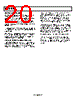
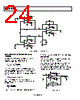
20 / 28 page  AD8065/AD8066 Rev. E | Page 20 of 28 THERMAL CONSIDERATIONS With 24 V power supplies and 6.5 mA quiescent current, the AD8065 dissipates 156 mW with no load. The AD8066 dissipates 312 mW. This can lead to noticeable thermal effects, especially in the small SOT-23-5 (thermal resistance of 160°C/W). VOS temperature drift is trimmed to guarantee a maximum drift of 17 µV/°C, so it can change up to 0.425 mV due to warm-up effects for an AD8065/AD8066 in a SOT-23-5 package on 24 V. Ib increases by a factor of 1.7 for every 10°C rise in temperature. Ib will be close to 5 times higher at 24 V supplies as opposed to a single 5 V supply. Heavy loads will increase power dissipation and raise the chip junction temperature as described in the Maximum Power Dissipation section. Care should be taken to not exceed the rated power dissipation of the package. INPUT AND OUTPUT OVERLOAD BEHAVIOR The AD8065/AD8066 have internal circuitry to guard against phase reversal due to overdriving the input stage. A simplified schematic of the input stage, including the input-protection diodes and antiphase reversal circuitry, is shown in Figure 56. The circuit is arranged such that when the input common- mode voltage exceeds a certain threshold, the input JFET pair’s bias current will turn OFF, and the bias current of an auxiliary NPN pair will turn ON, taking over control of the amplifier. When the input common-mode voltage returns to a viable operating value, the FET stage turns back ON, the NPN stage turns OFF, and normal operation resumes. The NPN pair can sustain operation with the input voltage up to the positive supply, so this is a pseudo rail-to-rail input stage. For operation beyond the FET stage’s common-mode limit, the amplifier’s VOS will change to the NPN pair’s offset (mean of 160 µV, standard deviation of 820 µV), and Ib will increase to the NPN pair’s base current up to 45 µA (see Figure 32). Switchback, or recovery time, is about 100 ns, see Figure 27. The output transistors of the rail-to-rail output stage have circuitry to limit the extent of their saturation when the output is overdriven. This helps output recovery time. Output recovery from a 0.5 V output overdrive on a ±5 V supply is shown in Figure 24. |
|
|
链接网址 |
| ALLDATASHEET是否为您带来帮助? [ DONATE ] |
关于 Alldatasheet | 广告服务 | 联系我们 | 隐私政策 | 数据表链接 | 链接交换 | 制造商名单 All Rights Reserved©Alldatasheet.com |
| Russian : Alldatasheetru.com | Korean : Alldatasheet.co.kr | Spanish : Alldatasheet.es | French : Alldatasheet.fr | Italian : Alldatasheetit.com Portuguese : Alldatasheetpt.com | Polish : Alldatasheet.pl | Vietnamese : Alldatasheet.vn Indian : Alldatasheet.in | Mexican : Alldatasheet.com.mx | British : Alldatasheet.co.uk | New Zealand : Alldatasheet.co.nz |
|
Family Site : ic2ic.com |
icmetro.com |
 Chinese ▼
 English
 Chinese
 German
 Japanese
 Russian
 Korean
 Spanish
 French
 Italian
 Portuguese
 Polish
 Vietnamese
 Indian
 Mexican
 British
 New Zealand