|
数据搜索系统,热门电子元器件搜索 |
|
|
数据搜索系统,热门电子元器件搜索 |
|
AD8626ARM-R2 数据表(PDF) 14 Page - Analog Devices |
|
|
|||||||||||||||||||||||||||||
AD8626ARM-R2 数据表(HTML) 14 Page - Analog Devices |
|
|
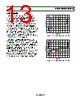
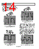
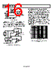
14 / 20 page  AD8627/AD8626/AD8625 Rev. B | Page 14 of 20 The AD862x can safely withstand input voltages 15 V below VSY if the total voltage between the positive supply and the input terminal is less than 26 V. Figure 41 through Figure 43 show the AD862x in different configurations accommodating signals close to the negative rail. The amplifier input stage typically maintains picoamp-level input currents across that input voltage range. TIME (2 µs/DIV) +5V 20k Ω 10k Ω 0V –2.5V VSY = 5V, 0V Figure 41. Gain of Two Inverter Response to 2.5 V Step, Centered –1.25 V below Ground TIME (2 µs/DIV) 5V 60mV 20mV 600 Ω 0V VSY = 5V RL = 600Ω Figure 42. Unity Gain Follower Response to 40 mV Step, Centered 40 mV above Ground TIME (2 µs/DIV) +5V 20k Ω 10k Ω –10mV –30mV 0V VSY = 5V Figure 43. Gain of Two Inverter Response to 20 mV Step, Centered 20 mV below Ground The AD862x is designed for 16 nV/√Hz wideband input voltage noise and maintains low noise performance to low frequencies, as shown in Figure 35. This noise performance, along with the AD862x’s low input current and current noise, means that the AD862x contributes negligible noise for applications with large source resistances. The AD862x has a unique bipolar rail-to-rail output stage that swings within 5 mV of the rail when up to 2 mA of current is drawn. At larger loads, the drop-out voltage increases as shown in Figure 17 and Figure 18. The AD862x’s wide bandwidth and fast slew rate allows it to be used with faster signals than previous single-supply JFETs. Figure 44 shows the response of AD862x, configured in unity gain, to a VIN of 20 V p-p at 50 kHz. The FPBW of the part is close to 100 kHz. TIME (5 µs/DIV) VSY = ±13V RL = 600Ω Figure 44. Unity Gain Follower Response to 20 V, 50 kHz Input Signal |
|
|
链接网址 |
| ALLDATASHEET是否为您带来帮助? [ DONATE ] |
关于 Alldatasheet | 广告服务 | 联系我们 | 隐私政策 | 数据表链接 | 链接交换 | 制造商名单 All Rights Reserved©Alldatasheet.com |
| Russian : Alldatasheetru.com | Korean : Alldatasheet.co.kr | Spanish : Alldatasheet.es | French : Alldatasheet.fr | Italian : Alldatasheetit.com Portuguese : Alldatasheetpt.com | Polish : Alldatasheet.pl | Vietnamese : Alldatasheet.vn Indian : Alldatasheet.in | Mexican : Alldatasheet.com.mx | British : Alldatasheet.co.uk | New Zealand : Alldatasheet.co.nz |
|
Family Site : ic2ic.com |
icmetro.com |
 Chinese ▼
 English
 Chinese
 German
 Japanese
 Russian
 Korean
 Spanish
 French
 Italian
 Portuguese
 Polish
 Vietnamese
 Indian
 Mexican
 British
 New Zealand