|
数据搜索系统,热门电子元器件搜索 |
|
|
数据搜索系统,热门电子元器件搜索 |
|
PL602-2XTC-R 数据表(PDF) 4 Page - Micrel Semiconductor |
|
|
|||||||||||||||||||||||||||||
PL602-2XTC-R 数据表(HTML) 4 Page - Micrel Semiconductor |
|
|
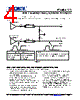
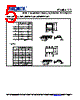
4 / 6 page  PL602-XX HCSL Compatible Clock Generator for PCI Express Micrel Inc. • 2180 Fortune Drive • San Jose, CA 95131 • USA • tel +1(408) 944 -0800 • fax +1(408) 474-1000 • www.micrel.com Rev 02/08/11 Page 4 PCI EXPRESS/HCSL COMPATIBLE LAYOUT GUIDELINES Figure 1 below describes how to terminate the complementary LVCMOS outputs of PL602-XX for use with HCSL inputs. 50 Ohm line 50 Ohm line Rs Rs Rt Rt LVCMOS Output Complementary LVCMOS Output 0V 3.3V 0V 0.75V Complementary Input Input Component Selection For 3.3V Operation Rs = 150 Ohm Rt = 50 Ohm Notes: Place Rs as close to the LVCMOS outputs as possible. Place Rt as close to the HCSL inputs as possible. HCSL Figure 1 For 2.5V Operation Rs = 100 Ohm Rt = 50 Ohm PCB LAYOUT CONSIDERATIONS FOR PERFORMANCE OPTIMIZATION The following guidelines are to assist you with a performance optimized PCB design: - Keep all the PCB traces to PL602-XX as short as possible, as well as keeping all other traces as far away from it as possible. - Place the crystal as close as possible to both crystal pins of the device. This will reduce the cross-talk between the crystal and the other signals. - Separate crystal pin traces from the other signals on the PCB, but allow ample distance between the two crystal pin traces. - Place a 0.01µF~0.1µF decoupling capacitor between VDD and GND, on the component side of the PCB, close to the VDD pin. It is not recommended to place this component on the backside of the PCB. - It is highly recommended to keep the VDD and GND traces as short as possible. - When connecting long traces (> 1 inch) to a CMOS output, it is important to design the traces as a transmission line or ‘stripline’, to avoid reflections or ringing. In this case, the CMOS output needs to be matched to the trace impedance. Usually ‘striplines’ are designed for 50Ω impedance and CMOS outputs usually have lower than 50Ω impedance so matching can be achieved by adding a resistor in series with the CMOS output pin to the ‘stripline’ trace. |
|
|
链接网址 |
| ALLDATASHEET是否为您带来帮助? [ DONATE ] |
关于 Alldatasheet | 广告服务 | 联系我们 | 隐私政策 | 数据表链接 | 链接交换 | 制造商名单 All Rights Reserved©Alldatasheet.com |
| Russian : Alldatasheetru.com | Korean : Alldatasheet.co.kr | Spanish : Alldatasheet.es | French : Alldatasheet.fr | Italian : Alldatasheetit.com Portuguese : Alldatasheetpt.com | Polish : Alldatasheet.pl | Vietnamese : Alldatasheet.vn Indian : Alldatasheet.in | Mexican : Alldatasheet.com.mx | British : Alldatasheet.co.uk | New Zealand : Alldatasheet.co.nz |
|
Family Site : ic2ic.com |
icmetro.com |
 Chinese ▼
 English
 Chinese
 German
 Japanese
 Russian
 Korean
 Spanish
 French
 Italian
 Portuguese
 Polish
 Vietnamese
 Indian
 Mexican
 British
 New Zealand