|
数据搜索系统,热门电子元器件搜索 |
|
|
数据搜索系统,热门电子元器件搜索 |
|
ADA4075-2ACPZ-R7 数据表(PDF) 19 Page - Analog Devices |
|
|
|||||||||||||||||||||||||||||
ADA4075-2ACPZ-R7 数据表(HTML) 19 Page - Analog Devices |
|
|
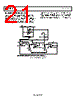
19 / 25 page  ADA4075-2 Data Sheet Rev. C | Page 18 of 24 BALANCED LINE DRIVER The circuit of Figure 67 shows a balanced line driver designed for audio use. Such drivers are intended to mimic an output transformer in operation, whereby the common-mode voltage can be impressed by the load. Furthermore, either output can be shorted to ground in single-ended applications without affecting the overall operation. Circuits of this type use positive and negative feedback to obtain a high common-mode output impedance, and they are somewhat notorious for component sensitivity and susceptibility to latch-up. This circuit uses several techniques to avoid spurious behavior. First, the 4-op-amp arrangement ensures that the input impedance is load independent (the input impedance can become negative with some configurations). Note that the output op amps are packaged with the input op amps to maximize drive capability. Second, the positive feedback is ac-coupled by C2 and C3, which eliminates the need for offset trim. Because the circuit is ac-coupled at the input, these capacitors do not have significant dc voltage across them, thus tantalum types of capacitors can be used. Finally, even with these precautions, it is vital that the positive feedback be accurately controlled. This is partly achieved by using 1% resistors. In addition, the following setup procedure ensures that the positive feedback does not become excessive: 1. Set R11 to its midposition (or short the ends together, whichever is easier) and temporarily short the negative output to ground. 2. Apply a 10 V p-p sine wave at approximately 1 kHz to the input and adjust R7 to provide 930 mV p-p at TEST (see Figure 67). 3. Remove the short from the negative output (and across R11, if used) and adjust R11 until the output waveforms are symmetric. The overall gain of the driver is equal to 2, which provides an extra 6 dB of headroom in balanced differential mode. The output noise is about −109 dBV in a 20 kHz bandwidth. C3 10µF R2 4.7k Ω OUT+ OUT– 1/2 ADA4075-2 R5 4.7k Ω R6 4.7k Ω R7 250Ω R8 100 Ω R9 4.7k Ω R13 100 Ω R4 4.7kΩ A2 1/2 ADA4075-2 A1 IN C5 50pF C1 10µF C2 10µF TEST SYMMETRY TRIM FEEDBACK TRIM 1/2 ADA4075-2 R12 4.7k Ω R11 250Ω R17 4.7k Ω R16 100 Ω R10 4.7k Ω R15 4.7k Ω A4 C6 50pF 1/2 ADA4075-2 A3 C4 50pF R14 100 Ω R1 10k Ω NOTES 1. ALL RESISTORS SHOULD HAVE 1% TOLERANCE. 2. A1/A2 IN SAME PACKAGE; A3/A4 IN SAME PACKAGE. R3 4.7k Ω R18 4.7k Ω Figure 67. Balanced Line Driver |
|
|
链接网址 |
| ALLDATASHEET是否为您带来帮助? [ DONATE ] |
关于 Alldatasheet | 广告服务 | 联系我们 | 隐私政策 | 数据表链接 | 链接交换 | 制造商名单 All Rights Reserved©Alldatasheet.com |
| Russian : Alldatasheetru.com | Korean : Alldatasheet.co.kr | Spanish : Alldatasheet.es | French : Alldatasheet.fr | Italian : Alldatasheetit.com Portuguese : Alldatasheetpt.com | Polish : Alldatasheet.pl | Vietnamese : Alldatasheet.vn Indian : Alldatasheet.in | Mexican : Alldatasheet.com.mx | British : Alldatasheet.co.uk | New Zealand : Alldatasheet.co.nz |
|
Family Site : ic2ic.com |
icmetro.com |
 Chinese ▼
 English
 Chinese
 German
 Japanese
 Russian
 Korean
 Spanish
 French
 Italian
 Portuguese
 Polish
 Vietnamese
 Indian
 Mexican
 British
 New Zealand