|
数据搜索系统,热门电子元器件搜索 |
|
|
数据搜索系统,热门电子元器件搜索 |
|
M24C64-RBN3P 数据表(PDF) 10 Page - STMicroelectronics |
|
|
|||||||||||||||||||||||||||||
M24C64-RBN3P 数据表(HTML) 10 Page - STMicroelectronics |
|
|
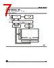
10 / 26 page  M24C64, M24C32 10/26 Page Write The Page Write mode allows up to 32 bytes to be written in a single Write cycle, provided that they are all located in the same ’row’ in the memory: that is, the most significant memory address bits (b12-b5 for M24C64, and b11-b5 for M24C32) are the same. If more bytes are sent than will fit up to the end of the row, a condition known as ‘roll-over’ occurs. This should be avoided, as data starts to become overwritten in an implementation depen- dent way. The bus master sends from 1 to 32 bytes of data, each of which is acknowledged by the device if Write Control (WC) is Low. If Write Control (WC) is High, the contents of the addressed memory loca- tion are not modified, and each data byte is fol- lowed by a NoAck. After each byte is transferred, the internal byte address counter (the 5 least sig- nificant address bits only) is incremented. The transfer is terminated by the bus master generat- ing a Stop condition. Figure 8. Write Mode Sequences with WC=0 (data write enabled) BYTE WRITE DEV SEL BYTE ADDR BYTE ADDR DATA IN WC PAGE WRITE DEV SEL BYTE ADDR BYTE ADDR DATA IN 1 WC DATA IN 2 AI01106C PAGE WRITE (cont'd) WC (cont'd) DATA IN N ACK R/W ACK ACK ACK ACK ACK ACK ACK R/W ACK ACK |
|
|
链接网址 |
| ALLDATASHEET是否为您带来帮助? [ DONATE ] |
关于 Alldatasheet | 广告服务 | 联系我们 | 隐私政策 | 数据表链接 | 链接交换 | 制造商名单 All Rights Reserved©Alldatasheet.com |
| Russian : Alldatasheetru.com | Korean : Alldatasheet.co.kr | Spanish : Alldatasheet.es | French : Alldatasheet.fr | Italian : Alldatasheetit.com Portuguese : Alldatasheetpt.com | Polish : Alldatasheet.pl | Vietnamese : Alldatasheet.vn Indian : Alldatasheet.in | Mexican : Alldatasheet.com.mx | British : Alldatasheet.co.uk | New Zealand : Alldatasheet.co.nz |
|
Family Site : ic2ic.com |
icmetro.com |
 Chinese ▼
 English
 Chinese
 German
 Japanese
 Russian
 Korean
 Spanish
 French
 Italian
 Portuguese
 Polish
 Vietnamese
 Indian
 Mexican
 British
 New Zealand