|
数据搜索系统,热门电子元器件搜索 |
|
|
数据搜索系统,热门电子元器件搜索 |
|
LED6000 数据表(PDF) 37 Page - STMicroelectronics |
|
|
|||||||||||||||||||||||||||||
LED6000 数据表(HTML) 37 Page - STMicroelectronics |
|
|
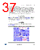
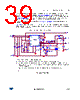
37 / 49 page  DocID027777 Rev 2 37/49 LED6000 Application notes - alternative topologies 49 This schematic also includes additional circuitry: A level shifter network for the proper dimming operation, since the LED6000 local ground (ICGND) is referred to the negative output voltage given by the voltage drop across the LEDs and the sensing resistor. This function is implemented by Q1, R15, R16 and R17. However, due to limited control loop bandwidth, the dimming operation in buck-boost topology is quite limited in terms of the minimum achievable DIM pulse. An external overvoltage protection which avoids the IC damage in case of the LED open row fault. This function is implemented by a Zener diode, D2, R7 and the sensing resistor, RSNS = R13. In case the LED string is disconnected the maximum output voltage is given by: Equation 31 Equation 31, in addition to Equation 27, must be verified in order avoid the LED6000 to be exposed to electrical stress outside the allowed range (seeTable 2 on page 7 for details). The series resistor, R7, must be selected in order to limit the maximum current flowing through the D2, as shown in Equation 32. Equation 32 The compensation network design strategy for buck-boost topology is described in Section 6.4 on page 44. Figure 24. Inverting buck-boost PCB layout (component side) 2 , D FB MAX OUT V V V 7 2 R R V I SNS FB D |
|
链接网址 |
| ALLDATASHEET是否为您带来帮助? [ DONATE ] |
关于 Alldatasheet | 广告服务 | 联系我们 | 隐私政策 | 数据表链接 | 链接交换 | 制造商名单 All Rights Reserved©Alldatasheet.com |
| Russian : Alldatasheetru.com | Korean : Alldatasheet.co.kr | Spanish : Alldatasheet.es | French : Alldatasheet.fr | Italian : Alldatasheetit.com Portuguese : Alldatasheetpt.com | Polish : Alldatasheet.pl | Vietnamese : Alldatasheet.vn Indian : Alldatasheet.in | Mexican : Alldatasheet.com.mx | British : Alldatasheet.co.uk | New Zealand : Alldatasheet.co.nz |
|
Family Site : ic2ic.com |
icmetro.com |
 Chinese ▼
 English
 Chinese
 German
 Japanese
 Russian
 Korean
 Spanish
 French
 Italian
 Portuguese
 Polish
 Vietnamese
 Indian
 Mexican
 British
 New Zealand