|
数据搜索系统,热门电子元器件搜索 |
|
|
数据搜索系统,热门电子元器件搜索 |
|
M93C76-R 数据表(PDF) 22 Page - STMicroelectronics |
|
|
|||||||||||||||||||||||||||||
M93C76-R 数据表(HTML) 22 Page - STMicroelectronics |
|
|
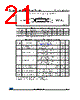
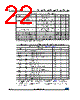
22 / 35 page  DC and AC parameters M93C86-x M93C76-x M93C66-x M93C56-x M93C46-x 22/35 DocID4997 Rev 17 Table 15. DC characteristics (M93Cx6-R) Symbol Parameter Test condition Min. Max. Unit ILI Input leakage current 0V ≤ VIN ≤ VCC - ±2.5 µA ILO Output leakage current 0V ≤ VOUT ≤ VCC, Q in Hi-Z - ±2.5 µA ICC Operating supply current VCC = 5 V, S = VIH, f = 2 MHz, Q = open - 2 mA VCC = 1.8 V, S = VIH, f = 1 MHz, Q = open - 1 mA ICC1 Standby supply current VCC = 1.8 V, S = VSS, C = VSS, ORG = VSS or VCC, pin7 = VCC, VSS or Hi-Z - 1(1) µA VIL Input low voltage (D, C, S) - –0.45 0.2 VCC V VIH Input high voltage (D, C, S) - 0.8 VCC VCC + 1 V VOL Output low voltage (Q) VCC = 1.8 V, IOL = 100 µA - 0.2 V VOH Output high voltage (Q) VCC = 1.8 V, IOH = –100 µA VCC–0.2 - V 1. 2 µA for previous devices identified with process letter G. Table 16. AC characteristics (M93Cx6-W, M93Cx6-R(1), device grade 6) 1. All M93Cx6-R devices operate with a clock frequency of 1MHz, as defined in Table 17. Only the new M93Cx6-R devices (identified with the process letter K) can operate with the 2 MHz timing values defined in this table. Test conditions specified in Table 8 and Table 12 Symbol Alt. Parameter Min. Max. Unit fC fSK Clock frequency D.C. 2 MHz tSLCH Chip Select low to Clock high 50 - ns tSHCH tCSS Chip Select setup time 50 - ns tSLSH (2) 2. Chip Select Input (S) must be brought low for a minimum of tSLSH between consecutive instruction cycles. tCS Chip Select low to Chip Select high 200 - ns tCHCL (3) 3. tCHCL + tCLCH ≥ 1 / fC. tSKH Clock high time 200 - ns tCLCH (3) tSKL Clock low time 200 - ns tDVCH tDIS Data in setup time 50 - ns tCHDX tDIH Data in hold time 50 - ns tCLSH tSKS Clock setup time (relative to S) 50 - ns tCLSL tCSH Chip Select hold time 0 - ns tSHQV tSV Chip Select to READY/BUSY status - 200 ns tSLQZ tDF Chip Select low to output Hi-Z - 100 ns tCHQL tPD0 Delay to output low - 200 ns tCHQV tPD1 Delay to output valid - 200 ns tW tWP Erase or Write cycle time - 5 ms |
|
链接网址 |
| ALLDATASHEET是否为您带来帮助? [ DONATE ] |
关于 Alldatasheet | 广告服务 | 联系我们 | 隐私政策 | 数据表链接 | 链接交换 | 制造商名单 All Rights Reserved©Alldatasheet.com |
| Russian : Alldatasheetru.com | Korean : Alldatasheet.co.kr | Spanish : Alldatasheet.es | French : Alldatasheet.fr | Italian : Alldatasheetit.com Portuguese : Alldatasheetpt.com | Polish : Alldatasheet.pl | Vietnamese : Alldatasheet.vn Indian : Alldatasheet.in | Mexican : Alldatasheet.com.mx | British : Alldatasheet.co.uk | New Zealand : Alldatasheet.co.nz |
|
Family Site : ic2ic.com |
icmetro.com |
 Chinese ▼
 English
 Chinese
 German
 Japanese
 Russian
 Korean
 Spanish
 French
 Italian
 Portuguese
 Polish
 Vietnamese
 Indian
 Mexican
 British
 New Zealand