|
数据搜索系统,热门电子元器件搜索 |
|
|
数据搜索系统,热门电子元器件搜索 |
|
M30620FCAFP 数据表(PDF) 239 Page - Mitsubishi Electric Semiconductor |
|
|
|||||||||||||||||||||||||||||
M30620FCAFP 数据表(HTML) 239 Page - Mitsubishi Electric Semiconductor |
|
|
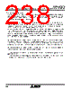
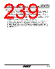
239 / 274 page  Appendix Standard Serial I/O Mode 1 (Flash Memory Version) Mitsubishi microcomputers M16C / 62A Group SINGLE-CHIP 16-BIT CMOS MICROCOMPUTER 239 Overview of standard serial I/O mode 1 (clock synchronized) In standard serial I/O mode 1, software commands, addresses and data are input and output between the MCU and peripheral units (serial programer, etc.) using 4-wire clock-synchronized serial I/O (UART1). Standard serial I/O mode 1 is engaged by releasing the reset with the P65 (CLK1) pin "H" level. In reception, software commands, addresses and program data are synchronized with the rise of the transfer clock that is input to the CLK1 pin, and are then input to the MCU via the RxD1 pin. In transmis- sion, the read data and status are synchronized with the fall of the transfer clock, and output from the TxD1 pin. The TxD1 pin is for CMOS output. Transfer is in 8-bit units with LSB first. When busy, such as during transmission, reception, erasing or program execution, the RTS1 (BUSY) pin is "H" level. Accordingly, always start the next transfer after the RTS1 (BUSY) pin is "L" level. Also, data and status registers in memory can be read after inputting software commands. Status, such as the operating state of the flash memory or whether a program or erase operation ended successfully or not, can be checked by reading the status register. Here following are explained software commands, status registers, etc. |
|
链接网址 |
| ALLDATASHEET是否为您带来帮助? [ DONATE ] |
关于 Alldatasheet | 广告服务 | 联系我们 | 隐私政策 | 数据表链接 | 链接交换 | 制造商名单 All Rights Reserved©Alldatasheet.com |
| Russian : Alldatasheetru.com | Korean : Alldatasheet.co.kr | Spanish : Alldatasheet.es | French : Alldatasheet.fr | Italian : Alldatasheetit.com Portuguese : Alldatasheetpt.com | Polish : Alldatasheet.pl | Vietnamese : Alldatasheet.vn Indian : Alldatasheet.in | Mexican : Alldatasheet.com.mx | British : Alldatasheet.co.uk | New Zealand : Alldatasheet.co.nz |
|
Family Site : ic2ic.com |
icmetro.com |
 Chinese ▼
 English
 Chinese
 German
 Japanese
 Russian
 Korean
 Spanish
 French
 Italian
 Portuguese
 Polish
 Vietnamese
 Indian
 Mexican
 British
 New Zealand