|
数据搜索系统,热门电子元器件搜索 |
|
|
数据搜索系统,热门电子元器件搜索 |
|
TUSB215RGYR 数据表(PDF) 9 Page - Texas Instruments |
|
|
|
|||||||||||||||||||||||||||||
TUSB215RGYR 数据表(HTML) 9 Page - Texas Instruments |
|
|
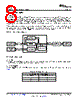
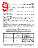
9 / 23 page  9 TUSB215 www.ti.com SLLSEX8A – AUGUST 2017 – REVISED AUGUST 2017 Product Folder Links: TUSB215 Submit Documentation Feedback Copyright © 2017, Texas Instruments Incorporated 7.3.3 BC1.2 CDP Support The TUSB215 main function is a signal conditioner offering the EQ/Boost features to the incoming DP/DM signals. For applications in which USB host or hub do not provide USB BC charging downstream port (CDP) functionality, the TUSB215 can perform this task. 7.4 Device Functional Modes 7.4.1 Low Speed (LS) Mode TUSB215 automatically detects a LS connection and does not enable signal compensation. CD pin is asserted high. 7.4.2 Full Speed (FS) Mode TUSB215 automatically detects a FS connection and does not enable signal compensation. CD pin is asserted high. 7.4.3 High Speed (HS) Mode TUSB215 automatically detects a HS connection and will enable signal compensation as determined by the configuration of the DC_BOOST pin and the external pulldown resistance on its EQ pin. CD pin asserted high. 7.4.4 Shutdown Mode TUSB215 is disabled when its RSTN pin is asserted low. In shutdown mode, the USB channel is still fully operational but there is neither signal compensation nor any indication from the CD pin as to the status of the channel. 7.4.5 I2C Mode TUSB215 support 100 kHz I2C for device configuration, status readback and test purposes. This controller is enabled after SCL and SDA pins are sampled high shortly after de-assertion of RSTN. In this mode, the register as described in Table 2 can be accessed by I2C read/write transaction to 7-bit slave address 0x2C. It is necessary to set CFG_ACTIVE bit and reset it to zero after making changes to the EQ and DC Boost level registers to restart the state machine. NOTE All registers or fields in Table 2 which are not specifically mentioned are considered reserved. The default value of these reserved registers or fields must not be changed. It is suggested to perform a read-modify-write operation to maintain the default value of the reserved fields. Table 2. Register definition Offset Bit(s) Name Type Default Description 0x01 6:4 ACB_LVL RW XXX (Sampled from EQ pin at reset) Sets the level of AC boost 000 :Level 0 AC boost programmed [MIN] 001 : Level 1 AC boost programmed 011 : Level 2 AC boost programmed 111 : Level 3 AC boost programmed [MAX] 0x03 0 CFG_ACTIVE RW 1b Configuration mode 0 : Normal mode. State machine enabled. 1 : Configuration mode: State machine disabled. After reset, if I2C mode is true (SCL and SDA are both pulled high) it is maintained until it is cleared by an I2C write, but, if I2C mode is not true, it is cleared automatically. |
|
|
链接网址 |
| ALLDATASHEET是否为您带来帮助? [ DONATE ] |
关于 Alldatasheet | 广告服务 | 联系我们 | 隐私政策 | 数据表链接 | 链接交换 | 制造商名单 All Rights Reserved©Alldatasheet.com |
| Russian : Alldatasheetru.com | Korean : Alldatasheet.co.kr | Spanish : Alldatasheet.es | French : Alldatasheet.fr | Italian : Alldatasheetit.com Portuguese : Alldatasheetpt.com | Polish : Alldatasheet.pl | Vietnamese : Alldatasheet.vn Indian : Alldatasheet.in | Mexican : Alldatasheet.com.mx | British : Alldatasheet.co.uk | New Zealand : Alldatasheet.co.nz |
|
Family Site : ic2ic.com |
icmetro.com |
 Chinese ▼
 English
 Chinese
 German
 Japanese
 Russian
 Korean
 Spanish
 French
 Italian
 Portuguese
 Polish
 Vietnamese
 Indian
 Mexican
 British
 New Zealand