|
数据搜索系统,热门电子元器件搜索 |
|
|
数据搜索系统,热门电子元器件搜索 |
|
UPC1663G 数据表(PDF) 2 Page - NEC |
|
|
|||||||||||||||||||||||||||||
UPC1663G 数据表(HTML) 2 Page - NEC |
|
|
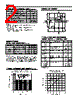
2 / 5 page  SYMBOLS PARAMETERS UNITS RATINGS VC–VE Voltage between VC and VE V -0.3 to 14 PT Total Power Dissipation2 mW 280 VID Differential Input Voltage V ±5 VIN Input Voltage V ±6 IO Output Current mA 35 TOP Operating Temperature °C -45 to +75 TSTG Storage Temperature °C -55 to +150 ABSOLUTE MAXIMUM RATINGS1 (TA = 25°C) EQUIVALENT CIRCUIT Supply Voltage, V ± (V) VIDEO LINE SINGLE ENDED OUTPUT VOLTAGE SWING vs. FREQUENCY Frequency, f (Hz) 2.0 1.0 0 100 k 1 M 10 M 100 M 1G OUT 75 Ω 75 Ω 75 Ω 75 Ω 200 Ω 200 Ω 0.1 µ VC = 6 V, Ve = -6 V TYPICAL PERFORMANCE UNDER SINGLE SUPPLY +5 V OPERATION* PARAMETER CONDITIONS TYPICAL UNITS Differential Gain 15 MHz Gain 1 35 dB Gain 2 11 dB Bandwidth Gain is 3 dB down from Gain 1 the gain at 100 KHz 106 MHz Gain 2 115 MHz Rise Time RS = 50 Ω, VOUT = 80 mVp-p Gain 1 2.2 ns Propagation Delay Gain 1 RS = 50 Ω, VOUT = 80 mVp-p 2.8 ns Gain 2 RS = 50 Ω, VOUT = 60 mVp-p 1.8 ns Phase Shift 100 MHz Gain 1 -123 degree Gain 2 -93 degree Output Power ZL = 50 Ω, 15 MHz RA = 240 Ω 5.0 dBm RA = 910 Ω 0 dBm RA = 80 Ω -11.5 dBm UPC1663G NORMALIZED VOLTAGE GAIN vs. SUPPLY VOLTAGE * See Application Circuit Notes: 1. Operation in excess of any one of these parameters may result in permanent damage. 2. Mounted on 5 cm x 5 cm x 0.16 mm glass epoxy PCB (TA = Max TOP). 3. Mounted on 50 cm x 50 cm x 1.6 mm glass epoxy PCB with copper film (TA = Max TOP). RECOMMENDED OPERATING CONDITIONS (TA = 25°C) SYMBOLS CHARACTERISTICS UNITS MIN TYP MAX VC Positive Supply Voltage V +2 +6 +6.5 Ve Negative Supply Voltage V -2 -6 -6.5 IO source Source Current mA 20 IO sink Sink Current mA 2.5 Frequency Range MHz DC 200 Attention: Due to high frequency characteristics, the physical circuit layout is very critical. Supply voltage line bypass, double-sided printed-circuit board, and wide-area ground line layout are necessary for stable operation. Two signal resistors connected to both inputs and two load resistors connected to both outputs should be balanced for stable operation. TYPICAL PERFORMANCE CURVES (TA = 25°C) 1.4 1.2 1.0 0.8 0.6 0.4 0.2 0.1 +2 +3 +4 +5 +6 +7 +8 VC Gain 2 Gain 1 -2 -3 -4 -5 -6 -7 -8 VE VC IN1 GA IN2 GB OUT1 OUT2 Ve |
|
|
链接网址 |
| ALLDATASHEET是否为您带来帮助? [ DONATE ] |
关于 Alldatasheet | 广告服务 | 联系我们 | 隐私政策 | 数据表链接 | 链接交换 | 制造商名单 All Rights Reserved©Alldatasheet.com |
| Russian : Alldatasheetru.com | Korean : Alldatasheet.co.kr | Spanish : Alldatasheet.es | French : Alldatasheet.fr | Italian : Alldatasheetit.com Portuguese : Alldatasheetpt.com | Polish : Alldatasheet.pl | Vietnamese : Alldatasheet.vn Indian : Alldatasheet.in | Mexican : Alldatasheet.com.mx | British : Alldatasheet.co.uk | New Zealand : Alldatasheet.co.nz |
|
Family Site : ic2ic.com |
icmetro.com |
 Chinese ▼
 English
 Chinese
 German
 Japanese
 Russian
 Korean
 Spanish
 French
 Italian
 Portuguese
 Polish
 Vietnamese
 Indian
 Mexican
 British
 New Zealand