|
数据搜索系统,热门电子元器件搜索 |
|
|
数据搜索系统,热门电子元器件搜索 |
|
AD8475ACPZ-R7 数据表(PDF) 19 Page - Analog Devices |
|
|
|||||||||||||||||||||||||||||
AD8475ACPZ-R7 数据表(HTML) 19 Page - Analog Devices |
|
|
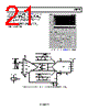
19 / 24 page  Data Sheet AD8475 Rev. D | Page 19 of 24 APPLICATIONS INFORMATION TYPICAL CONFIGURATION The AD8475 is designed to facilitate single-ended-to-differential conversion, common-mode level shifting, and precision attenuation of large signals so that they are compatible with low voltage ADCs. Figure 53 shows a typical connection diagram of the AD8475 in a gain of 0.4. To use the AD8475 in a gain of 0.8, drive the ±IN 0.8x inputs with a low impedance source. SINGLE-ENDED TO DIFFERENTIAL CONVERSION Many industrial systems use single-ended voltages in the signal path; however, the signals are frequently processed by high performance differential input ADCs for higher precision. The AD8475 performs the critical function of precisely converting single-ended signals to the differential inputs of precision ADCs, and it does so with no need for external components. To convert a single-ended signal to a differential signal, connect one input to the signal source and the other input to ground (see Figure 55). Note that either input can be driven by the source with the only effect being that the outputs have reversed polarity. The AD8475 also accepts truly differential input signals in precision systems with differential signal paths. SETTING THE OUTPUT COMMON-MODE VOLTAGE The VOCM pin of the AD8475 is internally biased with a precision voltage divider comprising two 200 kΩ resistors between the supplies. This divider level shifts the output to midsupply. Relying on the internal bias results in an output common-mode voltage that is within 0.01% of the expected value. In cases where control of the output common-mode level is desired, an external source with output resistance less than 100 Ω can be used to drive the VOCM pin. If an external voltage divider consisting of equal resistor values is used to set VOCM to midsupply, higher values can be used because the external resistors are placed in parallel with the internal resistors. The output common-mode gain error listed in the Specifications section assumes that the VOCM input is driven by a low impedance voltage source. Because of the internal divider, the VOCM pin sources and sinks current, depending on the externally applied voltage and its associated source resistance. It is also possible to connect the VOCM input to the voltage reference of an ADC via a resistor divider as shown in Figure 55. Connecting the VOCM input in this manner reduces power supply noise and optimizes the output common mode voltage of the AD8475 to utilize the entire differential input voltage range of the ADC. If AD8475 is used with a single supply that is the same voltage as the voltage reference, two 10 kΩ resistors connected to the VOCM pin is sufficient to override the inter- nal resistors. Otherwise, a voltage follower should be used to drive VOCM. VOUT = (V+OUT – V–OUT) 0.1µF REF +VS + 0.1µF 10µF LOW IMPEDANCE INPUT SOURCE –VS 0.1µF 10µF 1kΩ 1kΩ 1.25kΩ 1.25kΩ AD8475 –IN 0.8x –IN 0.4x +VS VOCM +OUT +IN 0.8x +IN 0.4x –VS NC –OUT 1.25kΩ 1.25kΩ Figure 52. Typical Configuration—10-Lead MSOP |
|
|
链接网址 |
| ALLDATASHEET是否为您带来帮助? [ DONATE ] |
关于 Alldatasheet | 广告服务 | 联系我们 | 隐私政策 | 数据表链接 | 链接交换 | 制造商名单 All Rights Reserved©Alldatasheet.com |
| Russian : Alldatasheetru.com | Korean : Alldatasheet.co.kr | Spanish : Alldatasheet.es | French : Alldatasheet.fr | Italian : Alldatasheetit.com Portuguese : Alldatasheetpt.com | Polish : Alldatasheet.pl | Vietnamese : Alldatasheet.vn Indian : Alldatasheet.in | Mexican : Alldatasheet.com.mx | British : Alldatasheet.co.uk | New Zealand : Alldatasheet.co.nz |
|
Family Site : ic2ic.com |
icmetro.com |
 Chinese ▼
 English
 Chinese
 German
 Japanese
 Russian
 Korean
 Spanish
 French
 Italian
 Portuguese
 Polish
 Vietnamese
 Indian
 Mexican
 British
 New Zealand