|
数据搜索系统,热门电子元器件搜索 |
|
|
数据搜索系统,热门电子元器件搜索 |
|
AD8027ART-R2 数据表(PDF) 16 Page - Analog Devices |
|
|
|||||||||||||||||||||||||||||
AD8027ART-R2 数据表(HTML) 16 Page - Analog Devices |
|
|
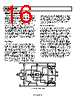
16 / 24 page  AD8027/AD8028 Rev. B | Page 16 of 24 THEORY OF OPERATION The AD8027/AD8028 is a rail-to-rail input and output amplifier designed in Analog Devices XFCB process. The XFCB process enables the AD8027/AD8028 to run on 2.7 V to 12 V supplies with 190 MHz of bandwidth and over 100 V/µs of slew rate. The AD8027/AD8028 has 4.3 nV/√Hz of wideband noise with 17 nV/√Hz noise at 10 Hz. This noise performance, with an offset and drift performance of less than 900 µV maximum and 1.5 µV/°C typical, respectively, makes the AD8027/AD8028 ideal for high speed precision applications. Additionally, the input stage operates 200 mV beyond the supply rails and shows no phase reversal. The amplifier features overvoltage protection on the input stage. Once the inputs exceed the supply rails by 0.7 V, ESD protection diodes will turn on, drawing excessive current through the differential input pins. A series input resis- tor should be included to limit the input current to less than 10 mA. Input Stage The rail-to-rail input performance is achieved by operating complementary input pairs. Which pair is on is determined by the common-mode level of the differential input signal. Look- ing at the schematic in Figure 55, a tail current (ITAIL) is gener- ated that sources the PNP differential input structure consisting of Q1 and Q2. A reference voltage is generated internally that is connected to the base of Q5. This voltage is continually com- pared against the common-mode input voltage. When the common-mode level exceeds the internal reference voltage, Q5 diverts the tail current (ITAIL) from the PNP input pair to a cur- rent mirror that sources the NPN input pair consisting of Q3 and Q4. The NPN input pair can now operate 200 mV above the positive rail. Both input pairs are protected from differential input signals above 1.4 V by four diodes across the input (see Figure 55). In the event of differential input signals that exceed 1.4 V, the diodes will conduct and excessive current will flow through them. A series input resistor should be included to limit the input current to 10 mA. Crossover Selection A new feature available on the AD8027/AD8028, which is called Crossover Selection, allows the user to choose the crossover point between the PNP/NPN differential pairs. Although the crossover region is small, operating in this region should be avoided since it can introduce offset and distortion to the out- put signal. To help avoid operating in the crossover region, the AD8027/AD8028 allows the user to select from two preset crossover locations (i.e., voltage levels) using the SELECT pin. Looking at the schematic in Figure 55, the crossover region is about 200 mV and is defined by the voltage level at the base of Q5. Internally, two separate voltage sources are created approxi- mately 1.2 V from either rail. One or the other is connected to Q5 based on the voltage applied to the SELECT pin. This allows for either dominant PNP pair operation, when the SELECT pin is left open, or dominant NPN pair operation, when the SELECT pin is pulled high. This pin also provides the tradi- tional power-down function when it is pulled low. This allows the designer to achieve the best precision and ac performance for high-side and low-side signal applications. See Figure 50 through Figure 53 for SELECT pin characteristics. VCC 1.2V + – VEE ITAIL 1.2V + – LOGIC VSEL VP Q5 Q3 Q1 Q2 Q4 VN VOUTP VOUTN ICMFB VCC VEE ICMFB 03327-A-054 Figure 55. Simplified Input Stage |
|
|
链接网址 |
| ALLDATASHEET是否为您带来帮助? [ DONATE ] |
关于 Alldatasheet | 广告服务 | 联系我们 | 隐私政策 | 数据表链接 | 链接交换 | 制造商名单 All Rights Reserved©Alldatasheet.com |
| Russian : Alldatasheetru.com | Korean : Alldatasheet.co.kr | Spanish : Alldatasheet.es | French : Alldatasheet.fr | Italian : Alldatasheetit.com Portuguese : Alldatasheetpt.com | Polish : Alldatasheet.pl | Vietnamese : Alldatasheet.vn Indian : Alldatasheet.in | Mexican : Alldatasheet.com.mx | British : Alldatasheet.co.uk | New Zealand : Alldatasheet.co.nz |
|
Family Site : ic2ic.com |
icmetro.com |
 Chinese ▼
 English
 Chinese
 German
 Japanese
 Russian
 Korean
 Spanish
 French
 Italian
 Portuguese
 Polish
 Vietnamese
 Indian
 Mexican
 British
 New Zealand