|
数据搜索系统,热门电子元器件搜索 |
|
|
数据搜索系统,热门电子元器件搜索 |
|
AD8566ARMZ-R2 数据表(PDF) 10 Page - Analog Devices |
|
|
|||||||||||||||||||||||||||||
AD8566ARMZ-R2 数据表(HTML) 10 Page - Analog Devices |
|
|
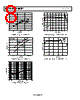
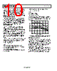
10 / 13 page  AD8565/AD8566/AD8567 Data Sheet Rev. H | Page 10 of 13 This input current is not inherently damaging to the device as long as it is limited to 5 mA or less. If a condition exists using the AD8565/AD8566/AD8567 where the input exceeds the supply more than 0.6 V, an external series resistor must be added. The size of the resistor can be calculated by using the maximum over-voltage divided by 5 mA. This resistance must be placed in series with either input exposed to an overvoltage. OUTPUT PHASE REVERSAL The AD8565/AD8566/AD8567 are immune to phase reversal. Although device output does not change phase, large currents due to input overvoltage could damage the device. In applica- tions where the possibility of an input voltage exceeding the supply voltage exists, overvoltage protection must be used as described in the Input Overvoltage Protection section. POWER DISSIPATION The maximum allowable internal junction temperature of 150°C limits the maximum power dissipation of AD8565/ AD8566/AD8567 devices. As the ambient temperature increases, the maximum power dissipated by AD8565/AD8566/ AD8567 devices must decrease linearly to maintain maximum junction temperature. If this maximum junction temperature is exceeded momentarily, the device still operates properly once the junction temperature is reduced below 150°C. If the maximum junction temperature is exceeded for an extended period, overheating could lead to permanent damage of the device. The maximum safe junction temperature, TJMAX, is 150°C. Using the following formula, the maximum power that an AD8565/ AD8566/AD8567 device can safely dissipate as a function of temperature can be obtained: PDISS = TJMAX − TA/θJA where: PDISS is the AD8565/AD8566/AD8567 power dissipation. TJMAX is the AD8565/AD8566/AD8567 maximum allowable junction temperature (150°C). TA is the ambient temperature of the circuit. θJA is the AD8565/AD8566/AD8567 package thermal resistance, junction-to-ambient. The power dissipated by the device can be calculated as PDISS = (VS − VOUT) × ILOAD where: VS is the supply voltage. VOUT is the output voltage. ILOAD is the output load current. Figure 30 shows the maximum power dissipation vs. temper- ature. To achieve proper operation, use the previous equation to calculate PDISS for a specific package at any given temperature or use Figure 30. AMBIENT TEMPERATURE (°C) 1.25 0.75 0 –35 0.50 0.25 1.00 –15 5 25 45 65 85 16-LEAD LFCSP 5-LEAD SC70 8-LEAD MSOP 14-LEAD TSSOP Figure 30. Maximum Power Dissipation vs. Temperature for 5-Lead SC70, 8-Lead MSOP, 14-Lead TSSOP, and 16-Lead LFCSP Packages THERMAL PAD—AD8567 The AD8567 LFCSP comes with a thermal pad that is attached to the substrate. This substrate is connected to the most positive supply, that is, Pin 3 in the LFCSP package and Pin 4 in the TSSOP package. To be electrically safe, the thermal pad must be soldered to an area on the board that is electrically isolated or connected to VDD. Attaching the thermal pad to ground adversely affects the performance of the part. Soldering down this thermal pad dramatically improves the heat dissipation of the package. It is necessary to attach vias that connect the soldered thermal pad to another layer on the board. This provides an avenue to dissipate the heat away from the part. Without vias, the heat is isolated directly under the part. |
|
|
链接网址 |
| ALLDATASHEET是否为您带来帮助? [ DONATE ] |
关于 Alldatasheet | 广告服务 | 联系我们 | 隐私政策 | 数据表链接 | 链接交换 | 制造商名单 All Rights Reserved©Alldatasheet.com |
| Russian : Alldatasheetru.com | Korean : Alldatasheet.co.kr | Spanish : Alldatasheet.es | French : Alldatasheet.fr | Italian : Alldatasheetit.com Portuguese : Alldatasheetpt.com | Polish : Alldatasheet.pl | Vietnamese : Alldatasheet.vn Indian : Alldatasheet.in | Mexican : Alldatasheet.com.mx | British : Alldatasheet.co.uk | New Zealand : Alldatasheet.co.nz |
|
Family Site : ic2ic.com |
icmetro.com |
 Chinese ▼
 English
 Chinese
 German
 Japanese
 Russian
 Korean
 Spanish
 French
 Italian
 Portuguese
 Polish
 Vietnamese
 Indian
 Mexican
 British
 New Zealand