|
数据搜索系统,热门电子元器件搜索 |
|
|
数据搜索系统,热门电子元器件搜索 |
|
AD8566ARMZ-R2 数据表(PDF) 11 Page - Analog Devices |
|
|
|||||||||||||||||||||||||||||
AD8566ARMZ-R2 数据表(HTML) 11 Page - Analog Devices |
|
|
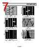
11 / 13 page  Data Sheet AD8565/AD8566/AD8567 Rev. H | Page 11 of 13 TOTAL HARMONIC DISTORTION + NOISE (THD + N) The AD8565/AD8566/AD8567 feature low total harmonic dis- tortion. Figure 31 shows THD + N vs. frequency. The THD + N over the entire supply range is below 0.008%. When the device is powered from a 16 V supply, the THD + N stays below 0.003%. Figure 31 shows the AD8566 in a unity noninverting configuration. FREQUENCY (Hz) 20 100 10 1 0.01 0.1 1k 10k 30k VS = ±2.5V VS = ±8V Figure 31. THD + N vs. Frequency SHORT-CIRCUIT OUTPUT CONDITIONS The AD8565/AD8566/AD8567 do not have internal short- circuit protection circuitry. As a precautionary measure, it is recommended not to short the output directly to the positive power supply or to ground. It is not recommended to operate the AD8565/AD8566/AD8567 with more than 35 mA of continuous output current. The output current can be limited by placing a series resistor at the output of the amplifier whose value can be derived using mA 35 S X V R For a 5 V single-supply operation, RX must have a minimum value of 143 Ω. LCD PANEL APPLICATIONS The AD8565/AD8566/AD8567 amplifier is designed for LCD panel applications or applications where large capacitive load drive is required. It can instantaneously source/sink greater than 250 mA of current. At unity gain, it can drive 1 μF without compensation. This makes the AD8565/AD8566/AD8567 ideal for LCD VCOM driver applications. To evaluate the performance of the AD8565/AD8566/AD8567, a test circuit was developed to simulate the VCOM driver application for an LCD panel. Figure 32 shows the test circuit. Series capacitors and resistors connected to the output of the op amp represent the load of the LCD panel. The 300 Ω and 3 kΩ feedback resistors are used to improve settling time. This test circuit simulates the worst-case scenario for a VCOM. It drives a represented load that is connected to a signal switched symmet- rically around VCOM. Figure 33 shows a scope photo of the instantaneous output peak current capability of the AD8565/AD8566/AD8567. INPUT 0VTO 8V SQUARE WAVE WITH 15.6µs PULSE WIDTH 300Ω 3kΩ 10Ω 10Ω 10Ω 10Ω 10nF 10nF 10nF 10nF MEASURE CURRENT 4V 8V 10Ω TO 20Ω Figure 32. VCOM Test Circuit with Supply Voltage at 16 V TIME (2µs/DIV) CH 2 = 100mA/DIV CH 1 = 5V/DIV 10 0% 100 90 Figure 33. Scope Photo of the VCOM Instantaneous Peak Current |
|
|
链接网址 |
| ALLDATASHEET是否为您带来帮助? [ DONATE ] |
关于 Alldatasheet | 广告服务 | 联系我们 | 隐私政策 | 数据表链接 | 链接交换 | 制造商名单 All Rights Reserved©Alldatasheet.com |
| Russian : Alldatasheetru.com | Korean : Alldatasheet.co.kr | Spanish : Alldatasheet.es | French : Alldatasheet.fr | Italian : Alldatasheetit.com Portuguese : Alldatasheetpt.com | Polish : Alldatasheet.pl | Vietnamese : Alldatasheet.vn Indian : Alldatasheet.in | Mexican : Alldatasheet.com.mx | British : Alldatasheet.co.uk | New Zealand : Alldatasheet.co.nz |
|
Family Site : ic2ic.com |
icmetro.com |
 Chinese ▼
 English
 Chinese
 German
 Japanese
 Russian
 Korean
 Spanish
 French
 Italian
 Portuguese
 Polish
 Vietnamese
 Indian
 Mexican
 British
 New Zealand