|
数据搜索系统,热门电子元器件搜索 |
|
|
数据搜索系统,热门电子元器件搜索 |
|
ADP2291ARMZ-R7 数据表(PDF) 13 Page - Analog Devices |
|
|
|||||||||||||||||||||||||||||
ADP2291ARMZ-R7 数据表(HTML) 13 Page - Analog Devices |
|
|
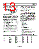
13 / 20 page  ADP2291 Rev. 0 | Page 13 of 20 In cases where the voltage drop across the protection device must be kept low, a P MOSFET is recommended. Connect the MOSFET as shown in Figure 21. ADP2291 RS INPUT 4.6V–12V IN CHG CIN CS DRV Figure 21. Reverse Input Protection EXTERNAL PASS TRANSISTOR Choose the external PNP pass transistor based on the given operating conditions and power handling capabilities. The pass device is determined by the base drive available, the input and output voltage, and the maximum charge current. Select the pass transistor with a collector-emitter breakdown voltage that exceeds the maximum adapter voltage. A VCEO rating of at least 15 V is recommended. To provide a charge current of IMAX with a minimum base drive of 40 mA requires a PNP beta of at least βMIN = mA I I I MAX MAX 40 = Β (5) Note that the beta of a transistor drops off with collector current. Therefore, make sure the beta at IMAX meets the minimum requirement. For cases where the adapter voltage is low (less than 5.5 V) calculate the saturation voltage using the following equation: VCE(SAT) = VADAPTER(MIN) − VPROTECT − VRS − VBAT (6) where VPROTECT = the forward drop of the reverse input protection. The power handling capabilities of the PNP pass transistor is another important parameter. The maximum power dissipation of the pass transistor is estimated using PDISS (W) = IMAX × (VADAPTER(MAX) − VPROTECT − VRS − VBAT) (7) where VRS = 150 mV at VADJ = 3.0 V = 50 mV at VADJ = 1.5 V VBAT = 2.8 V, the lowest cell voltage where fast charge can occur It should be noted that the adapter voltage can be either pre- regulated or unregulated. In the preregulated case the difference between the maximum and minimum adapter voltage is small. In this case use the maximum regulated adapter voltage to determine the maximum power dissipation. In the unregulated case, the adapter voltage can have a wide range specified. How- ever, the maximum voltage specified is usually with no load applied. Therefore, the worst-case power dissipation calculation often leads to an over-specified pass device. In either case, it is best to determine the load characteristics of the adapter to optimize the charger design. For example: VADAPTER(MIN) = 5.0 V VADAPTER(MAX) = 6.0 V IMAX = 500 mA VPROTECT = 0.2 V at 500 mA VADJ = 3 V VRS = 150 mV βMIN = 5 . 12 40 500 = = Β mA mA I IMAX VCE(SAT) = VADAPTER(MIN) − VPROTECT − VRS − VBAT = 5.0 V − 0.2 V − 0.15 V − 4.2 V = 0.45 V PDISS (W ) = IMAX × (VADAPTER(MAX) − VPROTECT − VRS − VBAT) = 0.50 A × (6.0 V − 0.2 V − 0.15 V − 2.8 V) = 1.4 W A guide for selecting the PNP transistor is given in Table 5. Table 5. PNP Pass Transistor Selection Guide Vendor Part Number Package Max PD@ 25°C Beta @1A VCE (SAT) Fairchild FSB6726 NZT45H8 SuperSOT SOT223 0.5 W 1.5 W 150 110 0.5 V 0.1 V ON Semi MTB35200 BCP53T1 MMJT9435 TSOP-6 SOT223 SOT223 0.625 W 1.5 W 1.6 W 200 35 200 0.175 V 0.3 V 0.18 V Philips BCP51 SOT223 1.3 W 50 0.5 V ZETEX ZXT10P20DE6 ZXT2M322 FZT549 FMMT549 SOT23-6 2 mm × 2 mm MLP SOT223 SOT23 1.1 W 1.5 W 2 W 0.5 W 270 270 130 130 0.17 V 0.17 V 0.25 V 0.25 V |
|
|
链接网址 |
| ALLDATASHEET是否为您带来帮助? [ DONATE ] |
关于 Alldatasheet | 广告服务 | 联系我们 | 隐私政策 | 数据表链接 | 链接交换 | 制造商名单 All Rights Reserved©Alldatasheet.com |
| Russian : Alldatasheetru.com | Korean : Alldatasheet.co.kr | Spanish : Alldatasheet.es | French : Alldatasheet.fr | Italian : Alldatasheetit.com Portuguese : Alldatasheetpt.com | Polish : Alldatasheet.pl | Vietnamese : Alldatasheet.vn Indian : Alldatasheet.in | Mexican : Alldatasheet.com.mx | British : Alldatasheet.co.uk | New Zealand : Alldatasheet.co.nz |
|
Family Site : ic2ic.com |
icmetro.com |
 Chinese ▼
 English
 Chinese
 German
 Japanese
 Russian
 Korean
 Spanish
 French
 Italian
 Portuguese
 Polish
 Vietnamese
 Indian
 Mexican
 British
 New Zealand