|
数据搜索系统,热门电子元器件搜索 |
|
|
数据搜索系统,热门电子元器件搜索 |
|
AD8099ACP-R2 数据表(PDF) 16 Page - Analog Devices |
|
|
|||||||||||||||||||||||||||||
AD8099ACP-R2 数据表(HTML) 16 Page - Analog Devices |
|
|
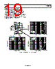
16 / 28 page  AD8099 Rev. B | Page 16 of 28 APPLICATIONS USING THE AD8099 The AD8099 offers unrivaled noise and distortion performance in low signal gain configurations. In low gain configurations (less than15), the AD8099 requires external compensation. The amount of gain and performance needed will determine the compensation network. Understanding the subtleties of the AD8099 gives the user insight on how to exact its peak performance. Use the component values and circuit configurations shown in the Applications section as starting points for designs. Specific circuit applications will dictate the final configuration and value of your components. CIRCUIT COMPONENTS The circuit components are referenced in Figure 59, the recommended noninverting circuit schematic for the AD8099. See Table 4 for typical component values and performance data. 1 8 4 7 5 3 6 2 AD8099 C5 0.1 µF CC CF C1 C4 10 µF C2 10 µF C3 0.1 µF RC RF RG RS R1 +VS –VS VOUT DISABLE VIN Figure 59. Wideband Noninverting Gain Configuration (SOIC) RF and RG — The feedback resistor and the gain set resistor determine the noise gain of the amplifier; typical RF values range from 250 Ω to 499 Ω. CF —Creates a zero in the loop response to compensate the pole created by the input capacitance (including stray capacitance) and the feedback resistor RF. CF helps reduce high frequency peaking and ringing in the closed-loop response. Typical range is 0.5 pF to 1.5 pF for evaluation circuits used here. R1 —This resistor terminates the input of the amplifier to the source resistance of the signal source, typically 50 Ω. (This is application specific and not always required.) RS —Many high speed amplifiers in low gain configurations require that the input stage be terminated into a nominal impedance to maintain stability. The value of RS should be kept to 50 Ω or lower to maintain low noise performance. At higher gains, RS may be reduced or even eliminated. Typical range is 0 Ω to 50 Ω. CC —The compensation capacitor decreases the open-loop gain at higher frequencies where the phase is degrading. By decreas- ing the open-loop gain here, the phase margin is increased and the amplifier is stabilized. Typical range is 0 pF to 5 pF. The value of CC is gain dependent. RC— The series lead inductance of the package and the com- pensation capacitance (CC) forms a series resonant circuit. RC dampens this resonance and prevents oscillations. The recommended value of RC is 50 Ω for a closed-loop gain of 2. This resistor introduces a zero in the open-loop response and must be kept low so that this zero occurs at a higher frequency. The purpose of the compensation network is to decrease the open-loop gain. If the resistance becomes too large, the gain will be reduced to the resistor value, and not necessarily to 0 Ω, which is what a single capacitor would do over frequency. Typical value range is 0 Ω to 50 Ω. C1 —To lower the impedance of RC , C1 is placed in parallel with RC. C1 is not required, but greatly reduces peaking at low closed-loop gains. The typical value range is 0 pF to 2 pF. C2 and C3 —Bypass capacitors are connected between both supplies for optimum distortion and PSRR performance. These capacitors should be placed as close as possible to the supply pins of the amplifier. For C3, C5, a 0508 case size should be used. The 0508 case size offers reduced inductance and better frequency response. C4 and C2 —Electrolytic bypass capacitors. |
|
|
链接网址 |
| ALLDATASHEET是否为您带来帮助? [ DONATE ] |
关于 Alldatasheet | 广告服务 | 联系我们 | 隐私政策 | 数据表链接 | 链接交换 | 制造商名单 All Rights Reserved©Alldatasheet.com |
| Russian : Alldatasheetru.com | Korean : Alldatasheet.co.kr | Spanish : Alldatasheet.es | French : Alldatasheet.fr | Italian : Alldatasheetit.com Portuguese : Alldatasheetpt.com | Polish : Alldatasheet.pl | Vietnamese : Alldatasheet.vn Indian : Alldatasheet.in | Mexican : Alldatasheet.com.mx | British : Alldatasheet.co.uk | New Zealand : Alldatasheet.co.nz |
|
Family Site : ic2ic.com |
icmetro.com |
 Chinese ▼
 English
 Chinese
 German
 Japanese
 Russian
 Korean
 Spanish
 French
 Italian
 Portuguese
 Polish
 Vietnamese
 Indian
 Mexican
 British
 New Zealand