|
数据搜索系统,热门电子元器件搜索 |
|
|
数据搜索系统,热门电子元器件搜索 |
|
ADRF6780ACPZN-R2 数据表(PDF) 23 Page - Analog Devices |
|
|
|||||||||||||||||||||||||||||
ADRF6780ACPZN-R2 数据表(HTML) 23 Page - Analog Devices |
|
|
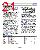
23 / 35 page  Data Sheet ADRF6780 Rev. D | Page 23 of 35 APPLICATIONS INFORMATION CARRIER FEEDTHROUGH NULLING Carrier feedthrough results from minute dc offsets that occur on the differential baseband inputs. In an I/Q modulator, nonzero differential offsets mix with the LO and result in carrier feedthrough to the RF output. In addition to this effect, some of the signal power at the LO input couples directly to the RF output (this may be because of the bond wire to bond wire coupling or coupling through the silicon substrate). The net carrier feedthrough at the RF output is the vector combination of the signals that appear at the output because of these two effects. A TxDAC can externally accomplish carrier feedthrough nulling. SIDEBAND SUPPRESSION OPTIMIZATION Sideband results from gain and phase imperfections between the I and Q channels. Sideband also results from the quadrature error in generating the quadrature LO signals. Quadrature I and Q signals are constructed in the LO path, and the vector combination of these signals at the RF output results in suppression of the unwanted sideband. Deviation from perfect quadrature on these signals limits the amount of achievable sideband suppression. The ADRF6780 offers quadrature phase adjustment in the LO path quadrature signals. Make these adjustments through the I_PATH_PHASE_ACCURACY bits (Register 0x05, Bits[3:0]) and Q_PATH_PHASE_ACCURACY (Register 0x05, Bits[7:4]) bits to reject the unwanted sideband signal. Figure 14 shows the level of unwanted sideband signal achievable from the ADRF6780 across the I_PATH_PHASE_ACCURACY bits (Register 0x05, Bits[3:0]) and Q_PATH_PHASE_ACCURACY (Register 0x05, Bits[7:4]) bits. If further optimization is needed, adjust the amplitude and phase externally through a TxDAC. LINEARITY The linearity in the ADRF6780 can be optimized through the distortion cancellation circuit that is set up by the RDAC_ LINEARIZE bits (Register 0x04, Bits[7:0]) SPI settings. The distortion cancellation circuit connects in parallel with the baseband signal path in such a way that the fundamental is minimally affected whereas the third-order portions cancel to some degree. Adjusting the value of the RDAC_LINEARIZE bits (Register 0x04, Bits[7:0]) changes the resistance value in the cancellation path by fine tuning the amount of third-order destructively added to the main signal path. It also serves as a form or predistortion for third-order impedance generated further down in the signal path. Figure 16 and Figure 44 show the level of linearity improvement achievable across the ADRF6780 RDAC_LINEARIZE bits. ADC The ADRF6780 includes an ADC that connects to a detector. The user has an option to read the detector output from the detector output pin (VDET, Pin 1) or using the ADC from the SPI. Figure 71 shows normal operation at I/Q mode, an RF output of 6.7 GHz, an I/Q input of 1 MHz, and a maximum gain. Figure 72 shows normal operation at IF mode and an RF output of 6.7 GHz, an IF input of 800 MHz, and a maximum gain. 0.05 0.25 0.45 0.65 0.85 1.05 1.25 0 50 100 150 200 250 300 RF OUTPUT POWER (dBm) ADC VALUE DETECTOR VOLTAGE(V) –35 –31 –27 –23 –19 –15 –11 –7 –3 1 Figure 71. ADC Detector Output and Detector Output Power, I/Q Mode 0.05 0.25 0.45 0.65 0.85 1.05 1.25 0 50 100 150 200 250 300 –35 –31 –27 –23 –19 –15 –11 –7 –3 1 RF OUTPUT POWER (dBm) ADC VALUE DETECTOR VOLTAGE (V) Figure 72. ADC Detector Output and Detector Output Power, IF Mode The following procedure is to read back from the detector for the first time. For each subsequent readback, repeat Step 4 to Step 8. To read back from the detector using the ADC, take the following steps: 1. Set Bit 7 of Register 0x03 to 1 (DETECTOR_ENABLE). 2. Set Bit 1 of Register 0x06 to 1 (ADC_ENABLE). Write 0x02 to Register 0x06. 3. Set Bit 0 of Register 0x06 to 1 (ADC_CLOCK_ENABLE). Write 0x03 to Register 0x06. 4. Set Bit 2 of Register 0x06 to 1 (ADC_START). Write 0x07 to Register 0x06. 5. Wait approximately 200 µs for the ADC to be ready. 6. Read back Bit 8 of Register 0x0C to 1 (ADC_STATUS). When the bit is high, proceed to Step 7. 7. Set Bit 2 of Register 0x06 to 0 (ADC_START). 8. Read back Bits[7:0] of Register 0x0C for the ADC value (ADC_VALUE). To disable the ADC, disable the ADC_CLOCK_ENABLE, ADC_ENABLE, and ADC_START bits. |
|
链接网址 |
| ALLDATASHEET是否为您带来帮助? [ DONATE ] |
关于 Alldatasheet | 广告服务 | 联系我们 | 隐私政策 | 数据表链接 | 链接交换 | 制造商名单 All Rights Reserved©Alldatasheet.com |
| Russian : Alldatasheetru.com | Korean : Alldatasheet.co.kr | Spanish : Alldatasheet.es | French : Alldatasheet.fr | Italian : Alldatasheetit.com Portuguese : Alldatasheetpt.com | Polish : Alldatasheet.pl | Vietnamese : Alldatasheet.vn Indian : Alldatasheet.in | Mexican : Alldatasheet.com.mx | British : Alldatasheet.co.uk | New Zealand : Alldatasheet.co.nz |
|
Family Site : ic2ic.com |
icmetro.com |
 Chinese ▼
 English
 Chinese
 German
 Japanese
 Russian
 Korean
 Spanish
 French
 Italian
 Portuguese
 Polish
 Vietnamese
 Indian
 Mexican
 British
 New Zealand