|
数据搜索系统,热门电子元器件搜索 |
|
|
数据搜索系统,热门电子元器件搜索 |
|
PLL701-21SC-R 数据表(PDF) 3 Page - PhaseLink Corporation |
|
|
|||||||||||||||||||||||||||||
PLL701-21SC-R 数据表(HTML) 3 Page - PhaseLink Corporation |
|
|
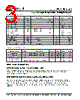
3 / 4 page  Preliminary PLL701-21 Low EMI Spread Spectrum Multiplier Clock 47745 Fremont Blvd., Fremont, California 94538 Tel (510) 492-0990 Fax (510) 492-0991 www.phaselink.com Rev 05/12/05 Page 3 2. DC/AC Specifications PARAMETERS SYMBOL CONDITIONS MIN. TYP. MAX. UNITS Supply Voltage VDD 2.97 3.63 V Input High Voltage VIH 0.7* VDD V Input Low Voltage VIL 0.3* VDD V Input High Current IIH 100 µA Input Low Current IIL 100 µA Output High Voltage VOH IOH=5mA, VDD =3.3V 2.4 V Output Low Voltage VOL IOL=6mA, VDD =3.3V 0.4 V Input Frequency FIN 24 200 MHz Maximum interruption of FIN 100 µs Input Capacitance Cin1 4 pF Pull-up Resistor Rpu PIN 2, 3, 7 30 k Ω Pull-down Resistor Rpd PIN 4 30 k Ω Short Circuit Current Isc 50 mA 3.3V Dynamic Supply Current ICC No Load 20 mA 3. TIMING CHARACTERISTICS PARAMETERS SYMBOL CONDITIONS MIN. TYP. MAX. UNITS Rise Time Tr Measured at 0.8V ~ 2.0V @ 3.3V 0.8 0.95 1.1 ns Fall Time Tf Measured at 2.0V ~ 0.8V @ 3.3V 0.78 0.85 0.9 ns Output Duty Cycle DT 45 50 55 % Input to Output Delay 2 4 ns Cycle to Cycle Jitter Tcyc-cyc Over output frequency range @ 3.3V 100 ps FUNCTIONAL DESCRIPTION Selectable spread spectrum and modulation rates The PLL701-21 provides Center Spread modulation, as well as a selectable modulation magnitude. Selection is made by connecting pins 2 (S2), 3 (S1) and 4 (S0) to a logical “zero” or “one”, according to the modulation magnitude selection table on page 1. Default values for S(0:3) through internal pull-up and pull-down resistor Selection pin 4 (S0) has an internal pull-down resistor of 30k Ω while pins 2, 3 and 7 (S2, S1 and S3) have an internal pull-up resistor of 30k Ω. This internal pull-down (or pull-up) resistor will pull the input value to a logical “zero” (or “one” respectively) by default, i.e. when no connection is made between the pin and VDD (GND respectively). In order to override the internal pull-down (pull-up), the pin has to be connected to VDD (GND respectively). |
|
|
链接网址 |
| ALLDATASHEET是否为您带来帮助? [ DONATE ] |
关于 Alldatasheet | 广告服务 | 联系我们 | 隐私政策 | 数据表链接 | 链接交换 | 制造商名单 All Rights Reserved©Alldatasheet.com |
| Russian : Alldatasheetru.com | Korean : Alldatasheet.co.kr | Spanish : Alldatasheet.es | French : Alldatasheet.fr | Italian : Alldatasheetit.com Portuguese : Alldatasheetpt.com | Polish : Alldatasheet.pl | Vietnamese : Alldatasheet.vn Indian : Alldatasheet.in | Mexican : Alldatasheet.com.mx | British : Alldatasheet.co.uk | New Zealand : Alldatasheet.co.nz |
|
Family Site : ic2ic.com |
icmetro.com |
 Chinese ▼
 English
 Chinese
 German
 Japanese
 Russian
 Korean
 Spanish
 French
 Italian
 Portuguese
 Polish
 Vietnamese
 Indian
 Mexican
 British
 New Zealand