|
数据搜索系统,热门电子元器件搜索 |
|
|
数据搜索系统,热门电子元器件搜索 |
|
STDRIVE601 数据表(PDF) 12 Page - STMicroelectronics |
|
|
|||||||||||||||||||||||||||||
STDRIVE601 数据表(HTML) 12 Page - STMicroelectronics |
|
|
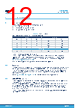
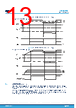
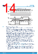
12 / 26 page  5 Functional description 5.1 Inputs and outputs The devices are controlled through the following logic inputs: • EN: Enable input, active high; • LIN: low-side driver inputs, active low; • HIN: high-side driver inputs, active low. Table 6. Inputs truth table Note: Applicable when device is not in UVLO or SmartSD protection Input pins Output pins EN LIN HIN LVG HVG L X X Low Low H H H Low Low H L H High Low H H L Low High Interlocking H L L Low Low The FAULT and OD pins are open-drain outputs. The FAULT signal is set low in case VCC UVLO is detected, or in case the SmartShutDown comparator triggers an event. It is only used to signal a UVLO or SmartSD activation to external circuits, and its state does not affect the behavior of other functions or circuits inside the driver. The OD behavior is explained in Section 5.5 Comparator and smart shutdown. When EN is set low, gate driver outputs are forced low and assure low impedance. 5.2 Deadtime The deadtime feature, in companion with interlocking feature, guarantees that driver outputs of the same channel are not high simultaneously and at least a DT time passes between the turn-off of one driver's output and the turn-on of the companion output of the same channel. If a deadtime longer than the internal DT is applied to LIN and HIN inputs by the external controller, the internal DT is ignored, and the outputs follow the deadtime determined by the inputs. Refer to Figure 4. Deadtime timing definitions for the dead time and interlocking waveforms. 5.3 VCC UVLO protection Undervoltage protection is available on VCC and BOOT supply pins. In order to avoid intermittent operation, a hysteresis set the turn-off threshold with respect to the turn-on threshold. When VCC voltage goes below VCCTHOFF threshold all the outputs are switched off, both LVG and HVG. When VCC voltage reaches VCCTHON threshold the driver returns to normal operation and sets the LVG outputs according to actual input pins status; HVG is also set according to input pin status if the corresponding VBO section is not in UVLO condition. The FAULT output is kept low when VCC is in UVLO condition. The following figures show some examples of typical operation conditions. STDRIVE601 Functional description DS12949 - Rev 2 page 12/26 |
|
|
链接网址 |
| ALLDATASHEET是否为您带来帮助? [ DONATE ] |
关于 Alldatasheet | 广告服务 | 联系我们 | 隐私政策 | 数据表链接 | 链接交换 | 制造商名单 All Rights Reserved©Alldatasheet.com |
| Russian : Alldatasheetru.com | Korean : Alldatasheet.co.kr | Spanish : Alldatasheet.es | French : Alldatasheet.fr | Italian : Alldatasheetit.com Portuguese : Alldatasheetpt.com | Polish : Alldatasheet.pl | Vietnamese : Alldatasheet.vn Indian : Alldatasheet.in | Mexican : Alldatasheet.com.mx | British : Alldatasheet.co.uk | New Zealand : Alldatasheet.co.nz |
|
Family Site : ic2ic.com |
icmetro.com |
 Chinese ▼
 English
 Chinese
 German
 Japanese
 Russian
 Korean
 Spanish
 French
 Italian
 Portuguese
 Polish
 Vietnamese
 Indian
 Mexican
 British
 New Zealand