|
数据搜索系统,热门电子元器件搜索 |
|
|
数据搜索系统,热门电子元器件搜索 |
|
AD8655ARMZ-R2 数据表(PDF) 16 Page - Analog Devices |
|
|
|||||||||||||||||||||||||||||
AD8655ARMZ-R2 数据表(HTML) 16 Page - Analog Devices |
|
|
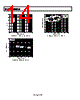
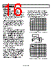
16 / 20 page  AD8655/AD8656 Rev. A | Page 16 of 20 APPLICATIONS INPUT OVERVOLTAGE PROTECTION One simple technique for compensation is a snubber that consists of a simple RC network. With this circuit in place, output swing is maintained, and the amplifier is stable at all gains. The internal protective circuitry of the AD8655/AD8656 allows voltages exceeding the supply to be applied at the input. It is recommended, however, not to apply voltages that exceed the supplies by more than 0.3 V at either input of the amplifier. If a higher input voltage is applied, series resistors should be used to limit the current flowing into the inputs. The input current should be limited to less than 5 mA. Figure 57 shows the implementation of a snubber, which reduces overshoot by more than 30% and eliminates ringing. Using a snubber does not recover the loss of bandwidth incurred from a heavy capacitive load. TIME (2 μs/DIV) VS = ±2.5V AV = 1 CL = 500pF The extremely low input bias current allows the use of larger resistors, which allows the user to apply higher voltages at the inputs. The use of these resistors adds thermal noise, which contributes to the overall output voltage noise of the amplifier. For example, a 10 kΩ resistor has less than 12.6 nV/√Hz of thermal noise and less than 10 nV of error voltage at room temperature. INPUT CAPACITANCE Along with bypassing and ground, high speed amplifiers can be sensitive to parasitic capacitance between the inputs and ground. For circuits with resistive feedback network, the total capacitance, whether it is the source capacitance, stray capacitance on the input pin, or the input capacitance of the amplifier, causes a breakpoint in the noise gain of the circuit. As a result, a capacitor must be added in parallel with the gain resistor to obtain stability. The noise gain is a function of frequency and peaks at the higher frequencies, assuming the feedback capaci- tor is selected to make the second-order system critically damped. A few picofarads of capacitance at the input reduce the input impedance at high frequencies, which increases the amplifier’s gain, causing peaking in the frequency response or oscillations. With the AD8655/AD8656, additional input damping is required for stability with capacitive loads greater than 200 pF with direct input to output feedback. See the Figure 56. Driving Heavy Capacitive Loads Without Compensation V+ 200 Ω 500pF 500pF V– VCC VEE 200mV + – + – Figure 57. Snubber Network VS = ±2.5V AV = 1 RS = 200Ω CS = 500pF CL = 500pF TIME (10 μs/DIV) Driving Capacitive Loads section. DRIVING CAPACITIVE LOADS Although the AD8655/AD8656 can drive capacitive loads up to 500 pF without oscillating, a large amount of ringing is present when operating the part with input frequencies above 100 kHz. This is especially true when the amplifiers are configured in positive unity gain (worst case). When such large capacitive loads are required, the use of external compensation is highly recommended. This reduces the overshoot and minimizes ringing, which, in turn, improves the stability of the AD8655/AD8656 when driving large capacitive loads. Figure 58. Driving Heavy Capacitive Loads Using a Snubber Network |
|
|
链接网址 |
| ALLDATASHEET是否为您带来帮助? [ DONATE ] |
关于 Alldatasheet | 广告服务 | 联系我们 | 隐私政策 | 数据表链接 | 链接交换 | 制造商名单 All Rights Reserved©Alldatasheet.com |
| Russian : Alldatasheetru.com | Korean : Alldatasheet.co.kr | Spanish : Alldatasheet.es | French : Alldatasheet.fr | Italian : Alldatasheetit.com Portuguese : Alldatasheetpt.com | Polish : Alldatasheet.pl | Vietnamese : Alldatasheet.vn Indian : Alldatasheet.in | Mexican : Alldatasheet.com.mx | British : Alldatasheet.co.uk | New Zealand : Alldatasheet.co.nz |
|
Family Site : ic2ic.com |
icmetro.com |
 Chinese ▼
 English
 Chinese
 German
 Japanese
 Russian
 Korean
 Spanish
 French
 Italian
 Portuguese
 Polish
 Vietnamese
 Indian
 Mexican
 British
 New Zealand