|
数据搜索系统,热门电子元器件搜索 |
|
|
数据搜索系统,热门电子元器件搜索 |
|
AD8031ARTZ-R2 数据表(PDF) 16 Page - Analog Devices |
|
|
|||||||||||||||||||||||||||||
AD8031ARTZ-R2 数据表(HTML) 16 Page - Analog Devices |
|
|
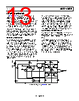
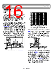
16 / 20 page  AD8031/AD8032 Data Sheet Rev. G | Page 16 of 20 APPLICATIONS A 2 MHz SINGLE-SUPPLY, BIQUAD BAND-PASS FILTER Figure 47 shows a circuit for a single-supply, biquad band-pass filter with a center frequency of 2 MHz. A 2.5 V bias level is easily created by connecting the noninverting inputs of all three op amps to a resistor divider consisting of two 1 kΩ resistors connected between 5 V and ground. This bias point is also decoupled to ground with a 0.1 µF capacitor. The frequency response of the filter is shown in Figure 48. To maintain an accurate center frequency, it is essential that the op amp have sufficient loop gain at 2 MHz. This requires the choice of an op amp with a significantly higher unity gain, crossover frequency. The unity gain, crossover frequency of the AD8031/AD8032 is 40 MHz. Multiplying the open-loop gain by the feedback factors of the individual op amp circuits yields the loop gain for each gain stage. From the feedback networks of the individual op amp circuits, it can be seen that each op amp has a loop gain of at least 21 dB. This level is high enough to ensure that the center frequency of the filter is not affected by the op amp’s bandwidth. If, for example, an op amp with a gain bandwidth product of 10 MHz was chosen in this application, the resulting center frequency would shift by 20% to 1.6 MHz. 5V 0.1µF 0.1µF 1k Ω 1k Ω AD8031 5V VOUT C2 50pF C1 50pF R6 1k Ω R4 2k Ω 1/2 AD8032 1/2 AD8032 R5 2k Ω R1 3k Ω VIN R2 2k Ω R3 2k Ω 0.1µF Figure 47. A 2 MHz, Biquad Band-Pass Filter Using AD8031/AD8032 FREQUENCY (Hz) –50 0 –10 –30 –40 –20 10k 100k 1M 10M 100M Figure 48. Frequency Response of 2 MHz Band-Pass Filter HIGH PERFORMANCE, SINGLE-SUPPLY LINE DRIVER Even though the AD8031/AD8032 swing close to both rails, the AD8031 has optimum distortion performance when the signal has a common-mode level half way between the supplies and when there is about 500 mV of headroom to each rail. If low distortion is required in single-supply applications for signals that swing close to ground, an emitter-follower circuit can be used at the op amp output. 10µF 5V 7 3 2 2N3904 200 Ω 6 2.49k Ω 49.9 Ω 4 AD8031 2.49k Ω 49.9 Ω 49.9 Ω 0.1µF VIN VOUT Figure 49. Low Distortion Line Driver for Single-Supply, Ground Referenced Signals Figure 49 shows the AD8031 configured as a single-supply, gain- of-2 line driver. With the output driving a back-terminated 50 Ω line, the overall gain from VIN to VOUT is unity. In addition to minimizing reflections, the 50 Ω back termination resistor protects the transistor from damage if the cable is short circuited. The emitter follower, which is inside the feedback loop, ensures that the output voltage from the AD8031 stays about 700 mV above ground. Using this circuit, low distortion is attainable even when the output signal swings to within 50 mV of ground. The circuit was tested at 500 kHz and 2 MHz. |
|
|
链接网址 |
| ALLDATASHEET是否为您带来帮助? [ DONATE ] |
关于 Alldatasheet | 广告服务 | 联系我们 | 隐私政策 | 数据表链接 | 链接交换 | 制造商名单 All Rights Reserved©Alldatasheet.com |
| Russian : Alldatasheetru.com | Korean : Alldatasheet.co.kr | Spanish : Alldatasheet.es | French : Alldatasheet.fr | Italian : Alldatasheetit.com Portuguese : Alldatasheetpt.com | Polish : Alldatasheet.pl | Vietnamese : Alldatasheet.vn Indian : Alldatasheet.in | Mexican : Alldatasheet.com.mx | British : Alldatasheet.co.uk | New Zealand : Alldatasheet.co.nz |
|
Family Site : ic2ic.com |
icmetro.com |
 Chinese ▼
 English
 Chinese
 German
 Japanese
 Russian
 Korean
 Spanish
 French
 Italian
 Portuguese
 Polish
 Vietnamese
 Indian
 Mexican
 British
 New Zealand