|
数据搜索系统,热门电子元器件搜索 |
|
|
数据搜索系统,热门电子元器件搜索 |
|
AD8031ARTZ-R2 数据表(PDF) 17 Page - Analog Devices |
|
|
|||||||||||||||||||||||||||||
AD8031ARTZ-R2 数据表(HTML) 17 Page - Analog Devices |
|
|
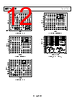
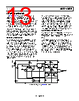
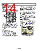
17 / 20 page  Data Sheet AD8031/AD8032 Rev. G | Page 17 of 20 Figure 50 and Figure 51 show the output signal swing and frequency spectrum at 500 kHz. At this frequency, the output signal (at VOUT), which has a peak-to-peak swing of 1.95 V (50 mV to 2 V), has a THD of −68 dB (SFDR = −77 dB). 2V 50mV 10 0% 100 90 0.5V 1µs Figure 50. Output Signal Swing of Low Distortion Line Driver at 500 kHz STOP 5MHz START 0Hz +9dBm Figure 51. THD of Low Distortion Line Driver at 500 kHz Figure 52 and Figure 53 show the output signal swing and frequency spectrum at 2 MHz. As expected, there is some degradation in signal quality at the higher frequency. When the output signal has a peak-to-peak swing of 1.45 V (swinging from 50 mV to 1.5 V), the THD is −55 dB (SFDR = −60 dB). This circuit could also be used to drive the analog input of a single-supply, high speed ADC whose input voltage range is referenced to ground (for example, 0 V to 2 V or 0 V to 4 V). In this case, a back termination resistor is not necessary (assuming a short physical distance from transistor to ADC); therefore, the emitter of the external transistor would be connected directly to the ADC input. The available output voltage swing of the circuit would therefore be doubled. 50mV 10 0% 100 90 1.5V 0.2V 200ns Figure 52. Output Signal Swing of Low Distortion Line Driver at 2 MHz +7dBm START 0Hz STOP 20MHz Figure 53. THD of Low Distortion Line Driver at 2 MHz |
|
|
链接网址 |
| ALLDATASHEET是否为您带来帮助? [ DONATE ] |
关于 Alldatasheet | 广告服务 | 联系我们 | 隐私政策 | 数据表链接 | 链接交换 | 制造商名单 All Rights Reserved©Alldatasheet.com |
| Russian : Alldatasheetru.com | Korean : Alldatasheet.co.kr | Spanish : Alldatasheet.es | French : Alldatasheet.fr | Italian : Alldatasheetit.com Portuguese : Alldatasheetpt.com | Polish : Alldatasheet.pl | Vietnamese : Alldatasheet.vn Indian : Alldatasheet.in | Mexican : Alldatasheet.com.mx | British : Alldatasheet.co.uk | New Zealand : Alldatasheet.co.nz |
|
Family Site : ic2ic.com |
icmetro.com |
 Chinese ▼
 English
 Chinese
 German
 Japanese
 Russian
 Korean
 Spanish
 French
 Italian
 Portuguese
 Polish
 Vietnamese
 Indian
 Mexican
 British
 New Zealand