|
数据搜索系统,热门电子元器件搜索 |
|
|
数据搜索系统,热门电子元器件搜索 |
|
LTC4150 数据表(PDF) 10 Page - Analog Devices |
|
|
|||||||||||||||||||||||||||||
LTC4150 数据表(HTML) 10 Page - Analog Devices |
|
|
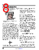
10 / 14 page  LT6106 10 Rev. C For more information www.analog.com APPLICATIONS INFORMATION power dissipation is 41mW. This amount of power dis- sipation will result in a 10°C rise in junction temperature above the ambient temperature. It is important to note that the LT6106 has been designed to provide at least 1mA to the output when required, and can deliver more depending on the conditions. Care must be taken to limit the maximum output current by proper choice of sense resistor and RIN– and, if input fault condi- tions exist, external clamps. Output Filtering The output voltage, VOUT, is simply IOUT • ZOUT. This makes filtering straightforward. Any circuit may be used which generates the required ZOUT to get the desired filter response. For example, a capacitor in parallel with ROUT will give a lowpass response. This will reduce unwanted noise from the output, and may also be useful as a charge reservoir to keep the output steady while driving a switch- ing circuit such as a MUX or ADC. This output capacitor in parallel with an output resistor will create a pole in the output response at: f–3dB = 1 2 • π •ROUT •COUT Useful Equations Input Voltage: VSENSE =ISENSE •RSENSE Voltage Gain: VOUT VSENSE = ROUT RIN Current Gain: IOUT ISENSE = RSENSE RIN Transconductance: IOUT VSENSE = 1 RIN Transimpedance: VOUT ISENSE = RSENSE • ROUT RIN Power Supply Connection For normal operation, the V+ pin should be connected to either side of the sense resistor. Either connection will meet the constraint that +IN ≤ V+ and –IN ≤ V+. During normal operation, VSENSE should not exceed 500mV (see VSENSE(MAX) under Electrical Characteristics). This ad- ditional constraint can be stated as V+ – (+IN) ≤ 500mV. Referring to Figure 5, feedback will force the voltages at the inputs –IN and +IN to be equal to (VS – VSENSE). Con- necting V+ to the load side of the shunt results in equal voltages at +IN, –IN and V+. Connecting V+ to the supply end of the shunt results in the voltages at +IN and –IN to be VSENSE below V+. If the V+ pin is connected to the supply side of the shunt resistor the supply current drawn by the LT6106 is not included in the monitored current. If the V+ pin is con- nected to the load side of the shunt resistor (Figure 5), the supply current drawn by the LT6106 is included in the monitored current. It should be noted that in either configuration, the output current of the LT6106 will not be monitored since it is drawn through the RIN resistor connected to the positive side of the shunt. Contact the factory for operation of the LT6106 with a V+ outside of the recommended operating range. Figure 5. LT6106 Supply Current Monitored with the Load Reverse Supply Protection Some applications may be tested with reverse-polarity supplies due to an expectation of the type of fault during operation. The LT6106 is not protected internally from externalreversalofsupplypolarity.Topreventdamagethat may occur during this condition, a Schottky diode should be added in series with V– (Figure 6). This will limit the reverse current through the LT6106. Note that this diode will limit the low voltage performance of the LT6106 by effectively reducing the supply voltage to the part by VD. LT6106 ROUT VOUT 6106 F05 RIN VS LOAD RSENSE V+ V– OUT –IN +IN |
|
|
链接网址 |
| ALLDATASHEET是否为您带来帮助? [ DONATE ] |
关于 Alldatasheet | 广告服务 | 联系我们 | 隐私政策 | 数据表链接 | 链接交换 | 制造商名单 All Rights Reserved©Alldatasheet.com |
| Russian : Alldatasheetru.com | Korean : Alldatasheet.co.kr | Spanish : Alldatasheet.es | French : Alldatasheet.fr | Italian : Alldatasheetit.com Portuguese : Alldatasheetpt.com | Polish : Alldatasheet.pl | Vietnamese : Alldatasheet.vn Indian : Alldatasheet.in | Mexican : Alldatasheet.com.mx | British : Alldatasheet.co.uk | New Zealand : Alldatasheet.co.nz |
|
Family Site : ic2ic.com |
icmetro.com |
 Chinese ▼
 English
 Chinese
 German
 Japanese
 Russian
 Korean
 Spanish
 French
 Italian
 Portuguese
 Polish
 Vietnamese
 Indian
 Mexican
 British
 New Zealand