|
数据搜索系统,热门电子元器件搜索 |
|
|
数据搜索系统,热门电子元器件搜索 |
|
LTC4150 数据表(PDF) 3 Page - Analog Devices |
|
|
|||||||||||||||||||||||||||||
LTC4150 数据表(HTML) 3 Page - Analog Devices |
|
|
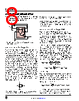
3 / 14 page  LT6106 3 Rev. C For more information www.analog.com Note 1: Stresses beyond those listed under Absolute Maximum Ratings may cause permanent damage to the device. Exposure to any Absolute Maximum Rating condition for extended periods may affect device reliability and lifetime. In addition to the Absolute Maximum Ratings, the output current of the LT6106 must be limited to insure that the power dissipation in the LT6106 does not allow the die temperature to exceed 150°C. See the Applications Information section “Power Dissipation Considerations” for further information. Note 2: Guaranteed by the gain error test. Note 3: Gain error refers to the contribution of the LT6106 internal circuitry and does not include errors in the external gain setting resistors. Note 4: The LT6106C is guaranteed functional over the operating temperature range of –40°C to 85°C. The LT6106C is designed, ELECTRICAL CHARACTERISTICS The l denotes the specifications which apply over the full specified operating temperature range, otherwise specifications are at TA = 25°C. V+ = 12V, V+ = VSENSE+, RIN = 100Ω, ROUT = 10k, Gain = 100 unless otherwise noted. SYMBOL PARAMETER CONDITIONS MIN TYP MAX UNITS VOUT(HIGH) Output Swing High (Referred to V+) VSENSE = 120mV l 1.2 1.4 V V Minimum Output Voltage (Note 5) VSENSE = 0mV, RIN = 100Ω, ROUT = 10k l 12 45 65 mV mV VSENSE = 0mV, RIN = 500Ω, ROUT = 10k, V+ = 12V, 36V l 7 16 22 mV mV BW Signal Bandwidth (–3dB) IOUT = 1mA, RIN = 100Ω, ROUT = 5k 200 kHz tr Input Step Response (to 50% of Output Step) ΔVSENSE = 100mV Step, RIN = 100Ω, ROUT = 5k, Rising Edge 3.5 µs IS Supply Current V+ = 2.7V, IOUT = 0µA, (VSENSE = –5mV) l 60 85 115 µA V+ = 12V, IOUT = 0µA, (VSENSE = –5mV) l 65 95 120 µA V+ = 36V, IOUT = 0µA, (VSENSE = –5mV) l 70 100 130 µA characterized and expected to meet specified performance from –40°C to 85°C but is not tested or QA sampled at these temperatures. The LT6106I is guaranteed to meet specified performance from –40°C to 85°C. The LT6106H is guaranteed to meet specified performance from –40°C to 125°C. Note 5: The LT6106 output is an open collector current source. The minimum output voltage scales directly with the ratio ROUT/10k. Note 6: VSENSE+ is the voltage at the high side of the sense resistor, RSENSE. See Figure 1. Note 7: VSENSE (MAX) is the maximum sense voltage for which the Electrical Characteristics will apply. Higher voltages can affect performance but will not damage the part provided that the output current of the LT6106 does not exceed the allowable power dissipation as described in Note 1. TYPICAL PERFORMANCE CHARACTERISTICS Input Offset Voltage vs Temperature TEMPERATURE (°C) –55 0 200 125 6106 G03 –200 –400 –25 5 35 65 95 400 –100 100 –300 300 VSENSE = 5mV V+ = 12V RIN = 100 ROUT = 10k AV = 100 TYPICAL UNITS INPUT OFFSET VOLTAGE (µV) –200 10 12 16 120 6106 G23 4 8 14 6 2 0 –120 –40 0 40 200 V+ = 12V VSENSE = 5mV RIN = 100 ROUT = 10k 1068 UNITS VOS Distribution SUPPLY VOLTAGE (V) 0 10 40 50 40 6106 G02 0 –10 –70 10 20 30 5 15 25 35 –30 70 60 30 20 –20 –40 –50 –60 VSENSE = 5mV RIN = 100 ROUT = 10k TYPICAL UNITS Input Offset Voltage vs Supply Voltage |
|
|
链接网址 |
| ALLDATASHEET是否为您带来帮助? [ DONATE ] |
关于 Alldatasheet | 广告服务 | 联系我们 | 隐私政策 | 数据表链接 | 链接交换 | 制造商名单 All Rights Reserved©Alldatasheet.com |
| Russian : Alldatasheetru.com | Korean : Alldatasheet.co.kr | Spanish : Alldatasheet.es | French : Alldatasheet.fr | Italian : Alldatasheetit.com Portuguese : Alldatasheetpt.com | Polish : Alldatasheet.pl | Vietnamese : Alldatasheet.vn Indian : Alldatasheet.in | Mexican : Alldatasheet.com.mx | British : Alldatasheet.co.uk | New Zealand : Alldatasheet.co.nz |
|
Family Site : ic2ic.com |
icmetro.com |
 Chinese ▼
 English
 Chinese
 German
 Japanese
 Russian
 Korean
 Spanish
 French
 Italian
 Portuguese
 Polish
 Vietnamese
 Indian
 Mexican
 British
 New Zealand