IP175C/IP175C LF/IP175CH/IP175CH LF
Data Sheet
31/111
Mar 09, 2007
Copyright © 2004, IC Plus Corp.
IP175C/IP175CH-DS-R14
Pin description (continued)
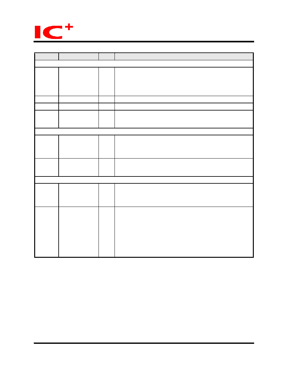
Pin No.
Label
Type
Description
Misc.
123
X1
I
System clock input or crystal input
It is recommended to connect X1 and X2 to a crystal. If the clock
source is from another chip, the clock should be active at least
for 1ms before pin 93 RESETB de-asserted.
122
X2
O
Crystal output
93
RESETB
I
Reset, low active
52
TEST2
IPL
Test mode enable
It should be connected to GND for normal operation.
EEPROM
53
SCL
IPL/O
After reset, it is used as clock pin SCL of EEPROM. Its period is
longer than 10us. IP175C/IP175CH stops reading EEPROM if it
finds there is no 55AA pattern in address 0. After reading
EEPROM, this pin becomes an input pin.
54
SDA
IPH/O After reset, it is used as data pin SDA of EEPROM. After reading
EEPROM, this pin becomes an input pin. It is pulled up in
24C01A application circuit.
SMI
71, 70
MDC0, MDIO0
IPL
SMI0
The external MAC device uses the interface to access
IP175C/IP175CH’s MII registers.
113, 74
MDC1, MDIO1
IPL/O
SMI1
IP175C/IP175CH uses the interface to polling the MII registers
of external PHY to get its status. It is active only if p4ext is pulled
high.
If the external PHY doesn’t support SMI, the polling result will be
16’hFFFF, and IP175C/IP175CH suppose the link status is
good.

 Chinese ▼
 English
 Chinese
 German
 Japanese
 Russian
 Korean
 Spanish
 French
 Italian
 Portuguese
 Polish
 Vietnamese
 Indian
 Mexican
 British
 New Zealand