|
数据搜索系统,热门电子元器件搜索 |
|
|
数据搜索系统,热门电子元器件搜索 |
|
SSM2250RMZ-R21 数据表(PDF) 8 Page - Analog Devices |
|
|
|||||||||||||||||||||||||||||
SSM2250RMZ-R21 数据表(HTML) 8 Page - Analog Devices |
|
|
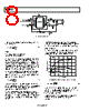
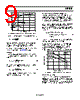
8 / 12 page  SSM2250 Rev. A | Page 8 of 12 NC NC NC LEFT IN RIGHT IN SHUTDOWN 5V BTL OUT 5V 100k Ω + – + 220 μF + 220 μF 1k Ω 1k Ω 1 μF 1 μF R1 20k Ω 10 μF R2 20k Ω R2 20k Ω R1 20k Ω SSM2250 5 14 1 2 3 4 13 12 11 10 6 7 9 8 NC NC = NO CONNECT NC Figure 14. Typical Application The output coupling capacitor creates a high-pass filter with a cutoff frequency of C L dB C R f π = − 2 1 3 (2) where: RL is the resistance of the headphone. CC is the output coupling capacitor. Although a majority of headphones have approximately 80 Ω of resistance, the resistance can vary between models and manu- facturers. Headphone resistances are commonly between 32 Ω to 600 Ω. Using a 220 μF capacitor, as shown in Figure 14, the worst-case −3 dB corner frequency would be 22 Hz, with a 32 Ω headphone load. Smaller output capacitors could be used at the expense of low frequency response to the headphones. An input coupling capacitor should be used to remove dc bias from the inputs to the SSM2250. Again, the input coupling capacitor in combination with the input resistor creates a high- pass filter with a corner frequency of 1 1 2 1 3 C R f dB π = − (3) Using the values shown in Figure 14, where R1 = 20 kΩ and C1 = 1 μF, creates a corner frequency of 8 Hz. This is acceptable, as the PC99 audio requirement specifies the computer audio system bandwidth to be 20 Hz to 20 kHz. Pin 10 on the SSM2250 provides the proper bias voltage for the amplifiers. A 0.1 μF capacitor should be connected here to reduce sensitivity to noise on the power supply. A larger capaci- tor can be used if more rejection from power supply noise is required. The SSM2250 has excellent phase margin and is stable even under heavy loading. Therefore, a feedback capacitor in parallel with R2 is not required, as it is in some competitors’ products. Power Dissipation An important advantage in using a bridged output configura- tion is that bridged output amplifiers are more efficient than single-ended amplifiers in delivering power to a load. OUTPUT POWER (W) 1.50 1.25 1.00 0.75 0.50 0.25 0 0 0.75 0.50 0.25 1.00 1.25 1.50 VDD = 5V RL = 4Ω RL = 16Ω RL = 8Ω Figure 15. Power Dissipation vs. Output Power in BTL Mode L DD MAX , DISS R V P 2 2 2 π = (4) Using Equation 4 and the power derating curve in Figure 17, the maximum ambient temperature can be easily found. This ensures that the SSM2250 does not exceed its maximum junction temperature of 150°C. The power dissipation for a single-ended output application where an output coupling capacitor is used is shown in Figure 16. |
|
|
链接网址 |
| ALLDATASHEET是否为您带来帮助? [ DONATE ] |
关于 Alldatasheet | 广告服务 | 联系我们 | 隐私政策 | 数据表链接 | 链接交换 | 制造商名单 All Rights Reserved©Alldatasheet.com |
| Russian : Alldatasheetru.com | Korean : Alldatasheet.co.kr | Spanish : Alldatasheet.es | French : Alldatasheet.fr | Italian : Alldatasheetit.com Portuguese : Alldatasheetpt.com | Polish : Alldatasheet.pl | Vietnamese : Alldatasheet.vn Indian : Alldatasheet.in | Mexican : Alldatasheet.com.mx | British : Alldatasheet.co.uk | New Zealand : Alldatasheet.co.nz |
|
Family Site : ic2ic.com |
icmetro.com |
 Chinese ▼
 English
 Chinese
 German
 Japanese
 Russian
 Korean
 Spanish
 French
 Italian
 Portuguese
 Polish
 Vietnamese
 Indian
 Mexican
 British
 New Zealand