|
数据搜索系统,热门电子元器件搜索 |
|
|
数据搜索系统,热门电子元器件搜索 |
|
OP1177ARM-R2 数据表(PDF) 18 Page - Analog Devices |
|
|
|||||||||||||||||||||||||||||
OP1177ARM-R2 数据表(HTML) 18 Page - Analog Devices |
|
|
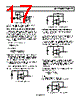
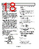
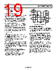
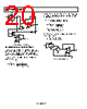
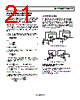
18 / 24 page  OP1177/OP2177/OP4177 Rev. E | Page 18 of 24 PROPER BOARD LAYOUT The OPx177 is a high precision device. To ensure optimum performance at the PCB level, care must be taken in the design of the board layout. To avoid leakage currents, the surface of the board should be kept clean and free of moisture. Coating the surface creates a barrier to moisture accumulation and helps reduce parasitic resistance on the board. Keeping supply traces short and properly bypassing the power supplies minimizes power supply disturbances due to output current variation, such as when driving an ac signal into a heavy load. Bypass capacitors should be connected as closely as possible to the device supply pins. Stray capacitances are a concern at the outputs and the inputs of the amplifier. It is recommended that signal traces be kept at least 5 mm from supply lines to minimize coupling. A variation in temperature across the PCB can cause a mismatch in the Seebeck voltages at solder joints and other points where dissi- milar metals are in contact, resulting in thermal voltage errors. To minimize these thermocouple effects, orient resistors so heat sources warm both ends equally. Input signal paths should contain matching numbers and types of components, where possible to match the number and type of thermocouple junctions. For example, dummy components such as zero value resistors can be used to match real resistors in the opposite input path. Matching components should be located in close proximity and should be oriented in the same manner. Ensure leads are of equal length so that thermal conduction is in equilibrium. Keep heat sources on the PCB as far away from amplifier input circuitry as is practical. The use of a ground plane is highly recommended. A ground plane reduces EMI noise and also helps to maintain a constant temperature across the circuit board. DIFFERENCE AMPLIFIERS Difference amplifiers are used in high accuracy circuits to improve the common-mode rejection ratio (CMRR). R1 V1 V2 R3 = R1 R4 = R1 OP1177 2 3 = R4 R3 R2 R1 R2 100kΩ VOUT 6 7 4 V+ V– Figure 63. Difference Amplifier In the single instrumentation amplifier (see Figure 63), where R1 R2 R3 R4 = () 1 2 O V V R1 R2 V − = a mismatch between the ratio R2/R1 and R4/R3 causes the common-mode rejection ratio to be reduced. To better understand this effect, consider that, by definition, CM DM A A CMRR = where ADM is the differential gain and ACM is the common- mode gain. CM O CM DIFF O DM V V A V V A and = = () 2 1 CM 2 1 DIFF V V V V V V + = − = 2 1 and For this circuit to act as a difference amplifier, its output must be proportional to the differential input signal. From Figure 63, 2 1 O V R4 R3 R1 R2 V R1 R2 V 1 1 ⎥ ⎥ ⎥ ⎥ ⎦ ⎤ ⎢ ⎢ ⎢ ⎢ ⎣ ⎡ ⎟ ⎠ ⎞ ⎜ ⎝ ⎛ + ⎟ ⎠ ⎞ ⎜ ⎝ ⎛ + + ⎟ ⎠ ⎞ ⎜ ⎝ ⎛ − = Arranging terms and combining the previous equations yields R2R3 R4R1 R4R2 R3R2 R4R1 CMRR 2 2 2 − + + = (1) The sensitivity of CMRR with respect to the R1 is obtained by taking the derivative of CMRR, in Equation 1, with respect to R1. ⎟ ⎠ ⎞ ⎜ ⎝ ⎛ − + + − δ δ = δ δ R2R3 R1R4 R2R3 R2R4 R2R3 R1R4 R1R4 R1 R1 CMRR 2 2 2 2 2 () R1R4 R2R3 R1 CMRR 2 2 1 − = δ δ Assuming that R1 ≈ R2 ≈ R3 ≈ R4 ≈ R and R(1 − δ) < R1, R2, R3, R4 < R(1 + δ) the worst-case CMRR error arises when R1 = R4 = R(1 + δ) and R2 = R3 = R(1 − δ) |
|
|
链接网址 |
| ALLDATASHEET是否为您带来帮助? [ DONATE ] |
关于 Alldatasheet | 广告服务 | 联系我们 | 隐私政策 | 数据表链接 | 链接交换 | 制造商名单 All Rights Reserved©Alldatasheet.com |
| Russian : Alldatasheetru.com | Korean : Alldatasheet.co.kr | Spanish : Alldatasheet.es | French : Alldatasheet.fr | Italian : Alldatasheetit.com Portuguese : Alldatasheetpt.com | Polish : Alldatasheet.pl | Vietnamese : Alldatasheet.vn Indian : Alldatasheet.in | Mexican : Alldatasheet.com.mx | British : Alldatasheet.co.uk | New Zealand : Alldatasheet.co.nz |
|
Family Site : ic2ic.com |
icmetro.com |
 Chinese ▼
 English
 Chinese
 German
 Japanese
 Russian
 Korean
 Spanish
 French
 Italian
 Portuguese
 Polish
 Vietnamese
 Indian
 Mexican
 British
 New Zealand