|
数据搜索系统,热门电子元器件搜索 |
|
|
数据搜索系统,热门电子元器件搜索 |
|
OP1177ARM-R2 数据表(PDF) 19 Page - Analog Devices |
|
|
|||||||||||||||||||||||||||||
OP1177ARM-R2 数据表(HTML) 19 Page - Analog Devices |
|
|
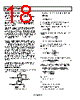
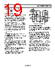
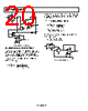
19 / 24 page  OP1177/OP2177/OP4177 Rev. E | Page 19 of 24 Plugging these values into Equation 1 yields δ ≅ 2 1 MIN CMRR where δ is the tolerance of the resistors. Lower tolerance value resistors result in higher common-mode rejection (up to the CMRR of the operational amplifier). Using 5% tolerance resistors, the highest CMRR that can be guaranteed is 20 dB. Alternatively, using 0.1% tolerance resistors results in a common-mode rejection ratio of at least 54 dB (assuming that the operational amplifier CMRR × 54 dB). With the CMRR of OPx177 at 120 dB minimum, the resistor match is the limiting factor in most circuits. A trimming resistor can be used to further improve resistor matching and CMRR of the difference amplifier circuit. A HIGH ACCURACY THERMOCOUPLE AMPLIFIER A thermocouple consists of two dissimilar metal wires placed in contact. The dissimilar metals produce a voltage VTC = α(TJ − TR) where: TJ is the temperature at the measurement of the hot junction. TR is the temperature at the cold junction. α is the Seebeck coefficient specific to the dissimilar metals used in the thermocouple. VTC is the thermocouple voltage and becomes larger with increasing temperature. Maximum measurement accuracy requires cold junction compen- sation of the thermocouple. To perform the cold junction compen- sation, apply a copper wire short across the terminating junctions (inside the isothermal block) simulating a 0°C point. Adjust the output voltage to zero using the R5 trimming resistor, and remove the copper wire. The OPx177 is an ideal amplifier for thermocouple circuits because it has a very low offset voltage, excellent PSRR and CMRR, and low noise at low frequencies. It can be used to create a thermocouple circuit with great linearity. Resistor R1, Resistor R2, and Diode D1, shown in Figure 64, are mounted in an isothermal block. V+ 7 4 Cu Cu TR TR D1 D1 ADR293 VCC C1 2.2µF R3 47kΩ 10µF R2 4.02kΩ R8 1kΩ R7 80.6kΩ R6 50Ω R9 200kΩ 0.1µF 10µF 0.1µF 10µF V– 10µF R4 50Ω R5 100Ω R1 50Ω ISOTHERMAL BLOCK VTC TJ (–) (+) 6 2 3 OP1177 VOUT Figure 64. Type K Thermocouple Amplifier Circuit LOW POWER LINEARIZED RTD A common application for a single element varying bridge is an RTD thermometer amplifier, as shown in Figure 65. The excita- tion is delivered to the bridge by a 2.5 V reference applied at the top of the bridge. RTDs may have thermal resistance as high as 0.5°C to 0.8°C per mW. To minimize errors due to resistor drift, the current through each leg of the bridge must be kept low. In this circuit, the amplifier supply current flows through the bridge. However, at the OPx177 maximum supply current of 600 μA, the RTD dissipates less than 0.1 mW of power, even at the highest resis- tance. Errors due to power dissipation in the bridge are kept under 0.1°C. Calibration of the bridge is made at the minimum value of temperature to be measured by adjusting RP until the output is zero. To calibrate the output span, set the full-scale and linearity potentiometers to midpoint and apply a 500°C temperature to the sensor or substitute the equivalent 500°C RTD resistance. Adjust the full-scale potentiometer for a 5 V output. Finally, apply 250°C or the equivalent RTD resistance and adjust the linearity potentiometer for 2.5 V output. The circuit achieves better than ±0.5°C accuracy after adjustment. |
|
|
链接网址 |
| ALLDATASHEET是否为您带来帮助? [ DONATE ] |
关于 Alldatasheet | 广告服务 | 联系我们 | 隐私政策 | 数据表链接 | 链接交换 | 制造商名单 All Rights Reserved©Alldatasheet.com |
| Russian : Alldatasheetru.com | Korean : Alldatasheet.co.kr | Spanish : Alldatasheet.es | French : Alldatasheet.fr | Italian : Alldatasheetit.com Portuguese : Alldatasheetpt.com | Polish : Alldatasheet.pl | Vietnamese : Alldatasheet.vn Indian : Alldatasheet.in | Mexican : Alldatasheet.com.mx | British : Alldatasheet.co.uk | New Zealand : Alldatasheet.co.nz |
|
Family Site : ic2ic.com |
icmetro.com |
 Chinese ▼
 English
 Chinese
 German
 Japanese
 Russian
 Korean
 Spanish
 French
 Italian
 Portuguese
 Polish
 Vietnamese
 Indian
 Mexican
 British
 New Zealand