|
数据搜索系统,热门电子元器件搜索 |
|
|
数据搜索系统,热门电子元器件搜索 |
|
OP2177ARM-R2 数据表(PDF) 15 Page - Analog Devices |
|
|
|||||||||||||||||||||||||||||
OP2177ARM-R2 数据表(HTML) 15 Page - Analog Devices |
|
|
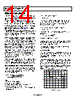
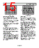
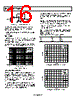
15 / 24 page  OP1177/OP2177/OP4177 Rev. E | Page 15 of 24 (5V/DIV) OPA277 VSY = ±15V RL = 2kΩ Figure 52. Gain Linearity INPUT OVERVOLTAGE PROTECTION When input voltages exceed the positive or negative supply voltage, most amplifiers require external resistors to protect them from damage. The OPx177 has internal protective circuitry that allows voltages as high as 2.5 V beyond the supplies to be applied at the input of either terminal without any harmful effects. Use an additional resistor in series with the inputs if the voltage exceeds the supplies by more than 2.5 V. The value of the resistor can be determined from the formula ( ) mA 5 500 ≤ Ω + − S S IN R V V With the OPx177 low input offset current of <1 nA maximum, placing a 5 kΩ resistor in series with both inputs adds less than 5 μV to input offset voltage and has a negligible impact on the overall noise performance of the circuit. 5 kΩ protects the inputs to more than 27 V beyond either supply. Refer to the THD + Noise section for additional information on noise vs. source resistance. OUTPUT PHASE REVERSAL Phase reversal is defined as a change of polarity in the amplifier transfer function. Many operational amplifiers exhibit phase reversal when the voltage applied to the input is greater than the maximum common-mode voltage. In some instances, this can cause permanent damage to the amplifier. In feedback loops, it can result in system lockups or equipment damage. The OPx177 is immune to phase reversal problems even at input voltages beyond the supplies. VSY = 10V AV = 1 TIME (400µs/DIV) VIN VOUT Figure 53. No Phase Reversal SETTLING TIME Settling time is defined as the time it takes an amplifier output to reach and remain within a percentage of its final value after application of an input pulse. It is especially important in measure- ment and control circuits in which amplifiers buffer ADC inputs or DAC outputs. To minimize settling time in amplifier circuits, use proper bypassing of power supplies and an appropriate choice of circuit components. Resistors should be metal film types, because they have less stray capacitance and inductance than their wire-wound counterparts. Capacitors should be polystyrene or polycarbonate types to minimize dielectric absorption. The leads from the power supply should be kept as short as possible to minimize capacitance and inductance. The OPx177 has a settling time of about 45 μs to 0.01% (1 mV) with a 10 V step applied to the input in a noninverting unity gain. OVERLOAD RECOVERY TIME Overload recovery is defined as the time it takes the output voltage of an amplifier to recover from a saturated condition to its linear response region. A common example is one in which the output voltage demanded by the transfer function of the circuit lies beyond the maximum output voltage capability of the amplifier. A 10 V input applied to an amplifier in a closed- loop gain of 2 demands an output voltage of 20 V. This is beyond the output voltage range of the OPx177 when operating at ±15 V supplies and forces the output into saturation. Recovery time is important in many applications, particularly where the operational amplifier must amplify small signals in the presence of large transient voltages. |
|
|
链接网址 |
| ALLDATASHEET是否为您带来帮助? [ DONATE ] |
关于 Alldatasheet | 广告服务 | 联系我们 | 隐私政策 | 数据表链接 | 链接交换 | 制造商名单 All Rights Reserved©Alldatasheet.com |
| Russian : Alldatasheetru.com | Korean : Alldatasheet.co.kr | Spanish : Alldatasheet.es | French : Alldatasheet.fr | Italian : Alldatasheetit.com Portuguese : Alldatasheetpt.com | Polish : Alldatasheet.pl | Vietnamese : Alldatasheet.vn Indian : Alldatasheet.in | Mexican : Alldatasheet.com.mx | British : Alldatasheet.co.uk | New Zealand : Alldatasheet.co.nz |
|
Family Site : ic2ic.com |
icmetro.com |
 Chinese ▼
 English
 Chinese
 German
 Japanese
 Russian
 Korean
 Spanish
 French
 Italian
 Portuguese
 Polish
 Vietnamese
 Indian
 Mexican
 British
 New Zealand