|
数据搜索系统,热门电子元器件搜索 |
|
|
数据搜索系统,热门电子元器件搜索 |
|
OP2177ARM-R2 数据表(PDF) 21 Page - Analog Devices |
|
|
|||||||||||||||||||||||||||||
OP2177ARM-R2 数据表(HTML) 21 Page - Analog Devices |
|
|
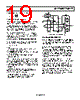
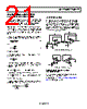
21 / 24 page  OP1177/OP2177/OP4177 Rev. E | Page 21 of 24 REALIZATION OF ACTIVE FILTERS BAND-PASS KRC OR SALLEN-KEY FILTER The low offset voltage and the high CMRR of the OPx177 make it an excellent choice for precision filters, such as the band-pass KRC filter shown in Figure 67. This filter type offers the capability to tune the gain and the cutoff frequency independently. Because the common-mode voltage into the amplifier varies with the input signal in the KRC filter circuit, a high CMRR is required to minimize distortion. Also, the low offset voltage of the OPx177 allows a wider dynamic range when the circuit gain is chosen to be high. The circuit of Figure 67 consists of two stages. The first stage is a simple high-pass filter where the corner frequency (fC) is C1C2R1R2 π 2 1 (2) and R2 R1 K Q = (3) where K is the dc gain. Choosing equal capacitor values minimizes the sensitivity and simplifies Equation 2 to R1R2 C π 2 1 The value of Q determines the peaking of the gain vs. frequency (ringing in transient response). Commonly chosen values for Q are generally near unity. Setting 2 1 Q = yields minimum gain peaking and minimum ringing. Determine values for R1 and R2 by using Equation 3. For , 2 1 Q = R1/R2 = 2 in the circuit example. Select R1 = 5 kΩ and R2 = 10 kΩ for simplicity. The second stage is a low-pass filter where the corner frequency can be determined in a similar fashion. For R3 = R4 = R C4 C3 Q C4 C3 πR f C 2 1 and 2 1 = = CHANNEL SEPARATION Multiple amplifiers on a single die are often required to reject any signals originating from the inputs or outputs of adjacent channels. OP2177 input and bias circuitry is designed to prevent feedthrough of signals from one amplifier channel to the other. As a result, the OP2177 has an impressive channel separation of greater than −120 dB for frequencies up to 100 kHz and greater than −115 dB for signals up to 1 MHz. C3 680pF 1/2 OP2177 7 8 6 5 4 V+ V– 1/2 OP2177 1 2 3 R2 10kΩ V1 + – R1 20kΩ C2 10nF C1 10nF R3 33kΩ R4 33kΩ C4 330pF VOUT Figure 67. Two-Stage, Band-Pass KRC Filter 1 2 3 1/2 OP2177 100Ω 10kΩ 1/2 OP2177 7 8 6 5 4 V+ V– + – V1 50mV Figure 68. Channel Separation Test Circuit REFERENCES ON NOISE DYNAMICS AND FLICKER NOISE S. Franco, Design with Operational Amplifiers and Analog Integrated Circuits. McGraw-Hill, 1998. Analog Devices, Inc., The Best of Analog Dialogue, 1967 to 1991. Analog Devices, Inc., 1991. |
|
|
链接网址 |
| ALLDATASHEET是否为您带来帮助? [ DONATE ] |
关于 Alldatasheet | 广告服务 | 联系我们 | 隐私政策 | 数据表链接 | 链接交换 | 制造商名单 All Rights Reserved©Alldatasheet.com |
| Russian : Alldatasheetru.com | Korean : Alldatasheet.co.kr | Spanish : Alldatasheet.es | French : Alldatasheet.fr | Italian : Alldatasheetit.com Portuguese : Alldatasheetpt.com | Polish : Alldatasheet.pl | Vietnamese : Alldatasheet.vn Indian : Alldatasheet.in | Mexican : Alldatasheet.com.mx | British : Alldatasheet.co.uk | New Zealand : Alldatasheet.co.nz |
|
Family Site : ic2ic.com |
icmetro.com |
 Chinese ▼
 English
 Chinese
 German
 Japanese
 Russian
 Korean
 Spanish
 French
 Italian
 Portuguese
 Polish
 Vietnamese
 Indian
 Mexican
 British
 New Zealand