|
数据搜索系统,热门电子元器件搜索 |
|
|
数据搜索系统,热门电子元器件搜索 |
|
AD8616ARMZ-R21 数据表(PDF) 12 Page - Analog Devices |
|
|
|||||||||||||||||||||||||||||
AD8616ARMZ-R21 数据表(HTML) 12 Page - Analog Devices |
|
|
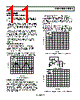
12 / 20 page  AD8615/AD8616/AD8618 Rev. C | Page 12 of 20 OVERLOAD RECOVERY TIME Overload recovery time is the time it takes the output of the amplifier to come out of saturation and recover to its linear region. Overload recovery is particularly important in applica- tions where small signals must be amplified in the presence of large transients. Figure 40 and Figure 41 show the positive and negative overload recovery times of the AD8616. In both cases, the time elapsed before the AD8616 comes out of saturation is less than 1 μs. In addition, the symmetry between the positive and negative recovery times allows excellent signal rectification without distortion to the output signal. TIME (1 μs/DIV) VS = ±2.5V RL = 10kΩ AV = 100 VIN = 50mV –50mV +2.5V 0V 0V Figure 40. Positive Overload Recovery TIME (1 μs/DIV) VS = ±2.5V RL = 10kΩ AV = 100 VIN = 50mV +50mV –2.5V 0V 0V Figure 41. Negative Overload Recovery D/A CONVERSION The AD8616 can be used at the output of high resolution DACs. Their low offset voltage, fast slew rate, and fast settling time make the parts suitable to buffer voltage output or current output DACs. Figure 42 shows an example of the AD8616 at the output of the AD5542. The AD8616’s rail-to-rail output and low distortion help maintain the accuracy needed in data acquisition systems and automated test equipment. AD5542 OUT UNIPOLAR OUTPUT AGND DGND REFS 1/2 AD8616 REFF VDD SERIAL INTERFACE 0.1 μF 0.1 μF 10 μF 5V 2.5V + CS DIN SCLK LDAC Figure 42. Buffering DAC Output LOW NOISE APPLICATIONS Although the AD8618 typically has less than 8 nV/√Hz of voltage noise density at 1 kHz, it is possible to reduce it fur- ther. A simple method is to connect the amplifiers in parallel, as shown in Figure 43. The total noise at the output is divided by the square root of the number of amplifiers. In this case, the total noise is approximately 4 nV/√Hz at room temperature. The 100 Ω resistor limits the current and provides an effective output resistance of 50 Ω. V– R3 100 Ω R1 10 Ω V+ VIN 3 2 1 R2 1k Ω V– R6 100 Ω R4 10 Ω V+ 3 2 1 R5 1k Ω V– R9 100 Ω R7 10 Ω V+ 3 2 1 R8 1k Ω V– R12 100 Ω R10 10 Ω V+ 3 2 1 R11 1k Ω VOUT Figure 43. Noise Reduction |
|
|
链接网址 |
| ALLDATASHEET是否为您带来帮助? [ DONATE ] |
关于 Alldatasheet | 广告服务 | 联系我们 | 隐私政策 | 数据表链接 | 链接交换 | 制造商名单 All Rights Reserved©Alldatasheet.com |
| Russian : Alldatasheetru.com | Korean : Alldatasheet.co.kr | Spanish : Alldatasheet.es | French : Alldatasheet.fr | Italian : Alldatasheetit.com Portuguese : Alldatasheetpt.com | Polish : Alldatasheet.pl | Vietnamese : Alldatasheet.vn Indian : Alldatasheet.in | Mexican : Alldatasheet.com.mx | British : Alldatasheet.co.uk | New Zealand : Alldatasheet.co.nz |
|
Family Site : ic2ic.com |
icmetro.com |
 Chinese ▼
 English
 Chinese
 German
 Japanese
 Russian
 Korean
 Spanish
 French
 Italian
 Portuguese
 Polish
 Vietnamese
 Indian
 Mexican
 British
 New Zealand