|
数据搜索系统,热门电子元器件搜索 |
|
|
数据搜索系统,热门电子元器件搜索 |
|
AD8260ACPZ-R7 数据表(PDF) 21 Page - Analog Devices |
|
|
|||||||||||||||||||||||||||||
AD8260ACPZ-R7 数据表(HTML) 21 Page - Analog Devices |
|
|
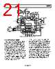
21 / 32 page  AD8260 Rev. 0 | Page 21 of 32 32 2 3 6 31 30 1.5kΩ 1kΩ 29 27 26 25 1kΩ 1.5kΩ GM 9 24 23 22 21 VMID 4 ×1 1 AD8260 VMDO TXEN VMDI VNCM VPSB ENBL VGAP VGAN VOCM INPP TXOP TXOP VPOS VPOS VPSR VMDO PRAI FDBK 50Ω 0.1µF 0.1µF 0V, 1.8V/3.3V 0V, 1.8V/3.3V 5 3.3V 7 8 0.1µF 0.1µF 1.8V OR 3.3V ADC FS INPUT 2V p-p INP INN 10 3.3V 11 12 13 14 16 15 17 18 19 RFB1 100Ω RFB2 100Ω 0.1µF 20 3.3V 0.1µF 0.1µF POWERLINE CABLE, ETC. OPTIONAL CLAMP DIODES AND SNUBBING RESISTORS 0.1µF 0.1µF 50Ω 1.8V OR 3.3V 20mA DAC 1V MAX WITH 200mA pk BIAS ATTENUATOR GM STAGES LOGIC 28 CFB OPTIONAL USER SELECTED CFB REDUCES HF PEAKING WITH CAPACITIVE LOADING LOW-PASS AA FILTER +– Figure 64. Block Diagram and Basic Application Connections HIGH CURRENT DRIVER AMPLIFIER The high current driver amplifier can deliver very large output currents suitable for driving complex impedances, such as a power line, a 50 Ω line, or a coaxial cable. The input of the amplifier is fully differential and intended to be driven by a differential current-output DAC, as shown in Figure 64. The differential input signal is amplified by 1.5× and produces a 2.25 V p-p single-ended output signal from a 1.5 V p-p input signal. A DAC with 15 mA maximum output current into a 50 Ω load provides 1.5 V p-p of input voltage and results in 2.25 V p-p at the output. A DAC whose output is 20 mA produces an output swing of 3 V p-p (neglecting a small gain error when driving the parallel combination of the 50 Ω load-resistor and the internal 1 kΩ gain resistor of the AD8260). For a 3.3 V supply rail, the maximum limit of the output voltage is 3 V p-p and distorts severely if exceeded. The recommended output for optimum distortion is 2 V p-p for a 3.3 V supply. Correspondingly, larger output swings are accommodated for higher supply voltages such as +5 V or ±5 V. For optimum distortion, the input drive must be controlled such that the output swing is well within saturation levels established by the supply rail. The output swing can be reduced by using load resistors with values less than 50 Ω or by reducing the amplifier gain by connecting external resistors in parallel with the internal 1 kΩ and 1.5 kΩ resistors between Pin 27, Pin 28, and Pin 29, and between Pin 30, Pin 31, and Pin 32. Coincidently, noise is reduced because the gain setting resistors are the primary noise sources of the high current driver amplifier. The output-referred noise is 14 nV/√Hz, of which 11 nV/√Hz is due to the gain setting resistors. Matching of the gain setting resistors is important for good common-mode rejection and the accuracy of the differential gain. If external resistors are used, their accuracy should be at least ±1%. How low the resistor values can be is primarily determined by the quality of the ac ground at Pin VOCM; as the gain setting resistors decrease in value, the dynamic current increases, and the quality of the decoupling capacitors needs to increase correspondingly. |
|
链接网址 |
| ALLDATASHEET是否为您带来帮助? [ DONATE ] |
关于 Alldatasheet | 广告服务 | 联系我们 | 隐私政策 | 数据表链接 | 链接交换 | 制造商名单 All Rights Reserved©Alldatasheet.com |
| Russian : Alldatasheetru.com | Korean : Alldatasheet.co.kr | Spanish : Alldatasheet.es | French : Alldatasheet.fr | Italian : Alldatasheetit.com Portuguese : Alldatasheetpt.com | Polish : Alldatasheet.pl | Vietnamese : Alldatasheet.vn Indian : Alldatasheet.in | Mexican : Alldatasheet.com.mx | British : Alldatasheet.co.uk | New Zealand : Alldatasheet.co.nz |
|
Family Site : ic2ic.com |
icmetro.com |
 Chinese ▼
 English
 Chinese
 German
 Japanese
 Russian
 Korean
 Spanish
 French
 Italian
 Portuguese
 Polish
 Vietnamese
 Indian
 Mexican
 British
 New Zealand