|
数据搜索系统,热门电子元器件搜索 |
|
|
数据搜索系统,热门电子元器件搜索 |
|
STV-366-R02 数据表(PDF) 6 Page - STMicroelectronics |
|
|
|||||||||||||||||||||||||||||
STV-366-R02 数据表(HTML) 6 Page - STMicroelectronics |
|
|
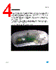
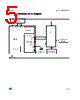
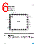
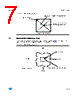
6 / 30 page  Design notes VT5366 6/30 3 Design notes 3.1 Pin assignment Figure 3. VT5366 pin assignment 3.2 Optical centre The optical centre of the VT5366 is NOT in the centre of the package, it is offset by - 0.243mm in the X-axis and 0.215mm in the Y axis with respect to the centre of the package as shown in Figure 4. The PCB designer must take this into account when laying out the PCB. 1 2 4 8 9 13 16 17 21 24 25 29 32 DVDD1 XI DVDD2 DGND2 NC TRK_LED NC NC TEST_OUT MOTION POWERDOWN SCL SDA NC XO VLEVEL VT5366 3 5 6 7 10 11 12 14 15 18 19 20 22 23 26 27 28 30 31 |
|
|
链接网址 |
| ALLDATASHEET是否为您带来帮助? [ DONATE ] |
关于 Alldatasheet | 广告服务 | 联系我们 | 隐私政策 | 数据表链接 | 链接交换 | 制造商名单 All Rights Reserved©Alldatasheet.com |
| Russian : Alldatasheetru.com | Korean : Alldatasheet.co.kr | Spanish : Alldatasheet.es | French : Alldatasheet.fr | Italian : Alldatasheetit.com Portuguese : Alldatasheetpt.com | Polish : Alldatasheet.pl | Vietnamese : Alldatasheet.vn Indian : Alldatasheet.in | Mexican : Alldatasheet.com.mx | British : Alldatasheet.co.uk | New Zealand : Alldatasheet.co.nz |
|
Family Site : ic2ic.com |
icmetro.com |
 Chinese ▼
 English
 Chinese
 German
 Japanese
 Russian
 Korean
 Spanish
 French
 Italian
 Portuguese
 Polish
 Vietnamese
 Indian
 Mexican
 British
 New Zealand